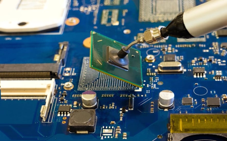
BGA Assembly is a specialized form of surface-mount technology (SMT) used to mount Ball Grid Array packages onto printed circuit boards. Unlike conventional leaded packages, BGA devices use an array of solder balls underneath the package to create electrical and mechanical connections with the PCB.
Because the solder joints are located underneath the component, they cannot be fully evaluated through conventional visual inspection after assembly. Precise component placement, controlled solder paste printing, optimized reflow profiles, and advanced inspection methods are therefore essential for reliable BGA PCB Assembly.
At Kingda, we support PCB assembly projects that use BGA packages and other high-density components. By combining controlled SMT processes with appropriate inspection and testing methods, manufacturers can improve assembly consistency, signal integrity, thermal performance, and long-term reliability.
What Is BGA Assembly?
BGA Assembly is the process of mounting a Ball Grid Array package onto a PCB using an array of solder balls as the electrical and mechanical connection points.
A typical BGA package consists of a semiconductor die, package substrate, interconnection structures, encapsulation or molding material, and an array of solder balls on the bottom surface. During assembly, the BGA package is positioned on corresponding PCB pads. The solder balls are then melted during the reflow process to form solder joints between the package and the PCB.
The BGA structure provides a large number of interconnections within a relatively small package footprint. This makes BGA packages particularly suitable for processors, memory devices, FPGAs, networking components, communication ICs, and other high-pin-count semiconductor devices.
Unlike through-hole components, BGA packages do not require leads to pass through drilled PCB holes. Instead, the connections are distributed across the underside of the package, allowing designers to achieve higher component density.

Common Types of BGA Packages
Different BGA package structures are available for different electrical, thermal, mechanical, and application requirements.
Plastic Ball Grid Array (PBGA)
PBGA packages generally use an organic substrate, often based on materials such as BT resin. The semiconductor die is connected to the package substrate through an internal interconnection method, while solder balls on the bottom provide the external connection to the PCB.
PBGA packages are widely used because they offer a practical balance between cost, package size, electrical performance, and manufacturing compatibility.
Ceramic Ball Grid Array (CBGA)
CBGA packages use a ceramic substrate instead of an organic package substrate.
Ceramic materials can provide excellent thermal stability and dimensional stability, making CBGA packages suitable for demanding applications where temperature cycling and environmental conditions are important considerations.
Tape Ball Grid Array (TBGA)
TBGA packages use a flexible tape or polyimide-based substrate. The package structure can be reinforced to provide sufficient mechanical stability.
TBGA technology can be used when a combination of thin package construction, high interconnection density, and electrical performance is required.
Other BGA Variants
Modern semiconductor packaging also includes package variations such as fine-pitch BGA, micro-BGA, flip-chip BGA, and other application-specific structures.
As BGA pitch becomes smaller, PCB fabrication and assembly tolerances become increasingly important. Fine-pitch packages require careful control of pad geometry, solder paste deposition, component placement, and reflow conditions.
Key Benefits of BGA Assembly
The popularity of BGA PCB Assembly comes from several important electrical, thermal, and mechanical advantages.
High Packaging Density
One of the most important benefits of BGA Components is their high I/O density.
Instead of using long leads around the perimeter of a package, BGA connections are distributed across the bottom surface. This allows more electrical connections to be accommodated within a relatively compact footprint.
The result is more efficient PCB space utilization, which is particularly valuable in computing, telecommunications, automotive electronics, and mobile devices.
Improved Electrical Performance
BGA packages generally have shorter electrical connection paths than many traditional leaded packages.
Shorter interconnections can reduce parasitic inductance and capacitance, which may help improve signal integrity at higher operating speeds. However, actual high-speed performance depends on the entire signal path, including the package, PCB stackup, routing, impedance control, vias, connectors, and power distribution network.
Good Thermal Performance
BGA packages provide multiple solder connections distributed underneath the package. Depending on the package structure and PCB design, these connections can contribute to heat transfer from the component into the PCB.
Thermal vias, copper planes, thermal pads, and appropriate PCB materials can further improve heat dissipation.
For high-power devices, thermal management should be evaluated as a complete system rather than relying solely on the BGA package.
Compact Component Size
BGA technology allows manufacturers to integrate a large number of electrical connections without requiring a large package perimeter.
This makes BGA packages well suited to compact electronic products where board space is limited.
Mechanical Reliability
The distributed solder-ball structure provides numerous connection points between the package and PCB.
When the package, PCB material, solder alloy, pad structure, and reflow process are properly selected, the resulting assembly can provide reliable electrical and mechanical performance.
However, BGA solder joints can be affected by thermal expansion differences between the package and PCB. Board thickness, material selection, component size, temperature cycling, and mechanical stress should therefore be considered during design.
BGA Assembly Process
A reliable SMT Assembly process for BGA components requires careful control from solder paste printing through final inspection.
Step 1: PCB and Material Preparation
Before assembly begins, the PCB and components should be verified against the approved bill of materials and manufacturing documentation.
Important checks include:
- PCB revision and dimensions
- Surface finish
- BGA pad geometry
- Solder mask design
- Component part number
- Package orientation
- BGA ball condition
- Moisture sensitivity requirements
- Storage conditions
BGA packages can be sensitive to moisture. Appropriate handling, storage, and preconditioning procedures should therefore be followed according to the component manufacturer’s requirements.
Step 2: Solder Paste Printing
Solder paste is printed onto the PCB pads using a stencil.
For BGA applications, solder paste deposition must be highly consistent because each individual solder joint contributes to the electrical and mechanical connection between the package and PCB.
Important process parameters include:
- Stencil thickness
- Aperture dimensions
- Aperture shape
- Squeegee pressure
- Printing speed
- Separation speed
- Paste viscosity
- PCB surface condition
The stencil design should be optimized for the BGA pitch, pad geometry, solder paste characteristics, and assembly process.
For many modern assemblies, lead-free alloys such as SAC305 are commonly used. The appropriate alloy should be selected according to the product requirements, component compatibility, and applicable manufacturing specifications.
BGA Pad Design: SMD vs. NSMD
The PCB pad design has a significant influence on BGA assembly reliability.
Solder Mask Defined (SMD) Pads
With solder mask defined pads, the solder mask opening is smaller than the underlying copper pad.
Part of the copper pad is covered by solder mask, which can provide additional mechanical reinforcement between the copper structure and PCB substrate.
SMD pads may be considered in applications where pad adhesion and mechanical robustness are important.
Non-Solder Mask Defined (NSMD) Pads
With non-solder mask defined pads, the solder mask opening is larger than the copper pad.
This exposes most or all of the copper pad surface and can provide a larger effective solderable area.
NSMD structures are commonly used for many BGA applications, but the appropriate pad design depends on the BGA package manufacturer’s recommendations, PCB fabrication capability, pitch, reliability requirements, and assembly process.
There is no universal rule that one pad structure is always superior. The design should be validated against the package land pattern and specific reliability requirements.
Step 3: BGA Component Placement
During placement, an automated pick-and-place machine accurately positions the BGA package onto the solder-pasted PCB.
The process generally includes:
- Component pickup from the feeder.
- Optical recognition of the package.
- Orientation and position correction.
- Placement onto the PCB.
- Verification of placement parameters.
High-precision placement is especially important for fine-pitch BGA packages.
BGA packages also exhibit a certain degree of self-alignment during reflow because surface tension of the molten solder can pull the component toward the center of the corresponding pad array. However, self-alignment should not be treated as a substitute for accurate placement.
Step 4: Reflow Soldering
Reflow Soldering is one of the most critical stages of the BGA assembly process.
The PCB passes through a controlled reflow oven where the solder paste is heated through several thermal zones. A typical reflow profile includes:
- Preheating
- Flux activation
- Thermal soaking
- Ramp-up
- Peak reflow
- Controlled cooling
The actual profile must be developed according to the solder alloy, PCB construction, component specifications, and thermal characteristics of the complete assembly.
Important parameters include peak temperature, time above liquidus, heating rate, cooling rate, and thermal uniformity across the PCB.
An unsuitable thermal profile may cause:
- Insufficient solder melting
- Poor wetting
- Solder bridging
- Excessive voiding
- Component warpage
- Pad or laminate damage
- Intermetallic-related reliability problems
For complex assemblies, thermocouples and thermal profiling equipment can be used to verify temperature behavior at representative locations on the PCB.
Step 5: Underfill Application
Some fine-pitch or mechanically demanding BGA applications may use underfill to improve board-level reliability.
Underfill material is dispensed into the space between the BGA package and PCB. After curing, the material can help distribute mechanical and thermal stresses across the package-to-board interface.
Underfill may be particularly useful when the assembly is exposed to significant temperature cycling, mechanical shock, vibration, or other reliability stresses.
Important underfill characteristics can include:
- Appropriate viscosity
- Good flow behavior
- Low void tendency
- Suitable coefficient of thermal expansion
- Appropriate glass transition temperature
- Strong adhesion
- Compatibility with the PCB and package materials
Not every BGA application requires underfill. The decision should be based on package construction, board design, reliability requirements, and the component manufacturer’s recommendations.
Step 6: BGA Inspection
Because BGA solder joints are located underneath the package, inspection requires techniques beyond conventional visual examination.
Automated Optical Inspection
AOI can inspect visible PCB features around the BGA area and verify component placement, orientation, solder paste-related indicators, and other accessible assembly characteristics.
However, conventional AOI cannot directly see most solder joints underneath the BGA package.
X-Ray Inspection
X-Ray Inspection is therefore particularly important for BGA assembly.
X-ray imaging can reveal hidden solder joints and help identify defects such as:
- Voids
- Bridging
- Insufficient solder
- Open solder joints
- Misalignment
- Abnormal solder-ball formation
For critical applications, 2D or 3D X-ray inspection may be used depending on the required level of analysis.
Void evaluation should follow appropriate acceptance criteria rather than relying on a single universal percentage. Acceptable voiding depends on component type, solder-joint geometry, thermal requirements, reliability specifications, and customer standards.

Common BGA Assembly Defects
BGA assembly defects can originate from PCB design, solder paste printing, component handling, placement, reflow, or material conditions.
Solder Bridging
Solder bridging occurs when molten solder creates an unintended electrical connection between adjacent pads.
Potential causes include excessive solder paste, inappropriate stencil apertures, insufficient spacing, or unsuitable reflow conditions.
Solder Voiding
Voids are gas-filled spaces within a solder joint.
Some level of voiding may occur naturally during reflow, but excessive or strategically located voids can affect thermal transfer, mechanical strength, or electrical performance.
Stencil design, solder paste selection, flux behavior, and reflow profile optimization can help control voiding.
Head-in-Pillow Defect
Head-in-pillow is a BGA-specific defect in which the solder ball and solder paste may melt separately without forming a reliable metallurgical connection.
It can be associated with package warpage, oxidation, insufficient solder paste contact, moisture-related package effects, or unsuitable reflow conditions.
This defect can be difficult to detect using conventional optical inspection and is one reason why process control and X-ray inspection are important for BGA manufacturing.
Open Solder Joints
An open solder joint occurs when the solder ball does not establish a continuous electrical and mechanical connection with the PCB pad.
Possible causes include:
- Insufficient solder paste
- Excessive component warpage
- Pad contamination
- Poor wetting
- Incorrect placement
- Thermal-profile problems
Component Warpage
BGA packages and PCBs can deform during heating because different materials have different coefficients of thermal expansion.
Excessive warpage can interfere with solder-joint formation and increase the risk of open connections.
How to Improve BGA Assembly Quality
High-quality PCB Assembly requires coordinated control of design, materials, equipment, and process parameters.
Optimize PCB Design
The PCB layout should consider:
- BGA pitch
- Pad dimensions
- Via placement
- Escape routing
- Solder mask design
- Copper distribution
- Thermal management
- Power integrity
- Signal integrity
For fine-pitch BGA packages, via-in-pad, microvias, and HDI structures may be considered when conventional fan-out routing cannot provide sufficient escape space.
Control Solder Paste Printing
Solder paste printing is often one of the most influential steps in BGA assembly.
Regular stencil inspection, solder paste management, SPI inspection, and optimized printing parameters can help maintain consistent paste volume and position.
Optimize Reflow Profiles
The reflow profile should be established based on the solder paste manufacturer’s recommendations and the thermal limitations of the components and PCB.
The goal is not simply to reach the highest possible temperature. Instead, the complete thermal profile must provide adequate solder melting and wetting while avoiding excessive thermal stress.
Use Appropriate Inspection Methods
A combination of SPI, AOI, X-ray inspection, and electrical testing can provide more comprehensive process coverage than any single inspection method.
For BGA assemblies, X-ray inspection is particularly valuable because many critical solder joints are hidden beneath the package.
BGA Assembly Applications
BGA packages are used across many electronic industries because they provide high I/O density, compact packaging, and good electrical performance.
Automotive Electronics
Automotive electronic systems increasingly use high-density semiconductor packages in applications such as advanced driver-assistance systems, infotainment, navigation, instrument clusters, communication modules, and control systems.
BGA technology can help integrate complex semiconductor functions into compact electronic modules.
Aerospace and Defense
Aerospace and defense electronics often require high functionality within limited space.
BGA packages can support high-density electronic designs, while thermal management, vibration resistance, environmental reliability, inspection, and manufacturing traceability must be carefully considered.
Industrial Equipment
Industrial control systems, instrumentation, motor drives, automation equipment, networking systems, and machine-vision platforms can use BGA-based semiconductor devices.
These applications may require reliable operation across temperature variation and long service periods.
Computers and Mobile Devices
Processors, memory devices, graphics components, communication ICs, and other high-performance semiconductor devices commonly use BGA packaging.
The compact structure enables manufacturers to integrate high processing capability into relatively small products.
Telecommunications and Networking
Routers, switches, wireless communication equipment, and other networking hardware often require high-density semiconductor packages.
The electrical characteristics and compact footprint of BGA packages make them suitable for high-speed digital and communication applications.
Why Choose Kingda for BGA Assembly?
Selecting a BGA assembly partner requires more than comparing the lowest quotation. Because BGA solder joints are small and largely hidden beneath the package, manufacturers need appropriate process controls, equipment, inspection capabilities, and engineering support.
When evaluating a supplier, consider the following factors:
Manufacturing and Assembly Capability
The supplier should have suitable SMT equipment for accurate placement of standard and fine-pitch BGA packages.
The manufacturing process should also support controlled solder paste printing, reflow profiling, inspection, and testing.
Inspection Capability
A reliable BGA assembly provider should have inspection methods appropriate for hidden solder joints.
Depending on product requirements, this may include SPI, AOI, X-ray inspection, and electrical testing.
Engineering and DFM Support
A capable supplier should be able to review BGA land patterns, PCB stackups, component placement, escape routing, thermal design, and manufacturability before production.
Early DFM analysis can identify potential assembly risks and reduce costly changes later in the project.
Quality and Process Control
BGA assembly quality depends on stable control of the entire process chain.
Material verification, solder paste management, placement accuracy, thermal profiling, inspection, testing, and production records should all be incorporated into an appropriate quality-management system.
Flexible Production Support
Different products have different requirements. Prototypes may require rapid engineering feedback and flexible rework, while production programs may require repeatable processes and stable quality.
A suitable supplier should be able to adapt its manufacturing and inspection strategy to the project’s product structure and production requirements.
BGA Assembly Services at Kingda
Kingda provides BGA Assembly solutions for electronic products that require high-density semiconductor packaging and reliable PCB integration.
Our approach focuses on process consistency, accurate component placement, controlled soldering, appropriate inspection, and manufacturability. BGA assembly can also be integrated with conventional SMT components, through-hole components, and other PCB assembly technologies when required by the product design.
For projects involving fine-pitch BGA packages, complex multilayer PCBs, high-density routing, or mixed-technology assembly, early cooperation between the PCB designer and manufacturing team can help identify potential risks before production.
Conclusion
BGA Assembly is an advanced SMT process that enables high-density semiconductor packages to be integrated into modern electronic products. Its compact footprint, high I/O density, short electrical connections, and potential thermal advantages make BGA technology suitable for computing, automotive, industrial, aerospace, telecommunications, and consumer electronics.
However, BGA assembly also introduces unique manufacturing challenges because the solder joints are located underneath the component and cannot be fully evaluated through conventional visual inspection.
Reliable results depend on accurate PCB pad design, consistent solder paste printing, precise placement, optimized Reflow Soldering, controlled material handling, and effective X-Ray Inspection. For demanding applications, additional measures such as underfill, advanced thermal management, and electrical testing may also be required.
By combining appropriate PCB design practices with controlled manufacturing and inspection processes, Kingda can support reliable BGA PCB Assembly for both development and production applications.