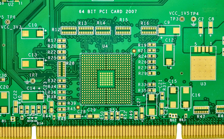
Ground Routing and Power Trace Planning Routing begins with a decision that is easy to postpone and expensive to revisit: where the ground and the power go. Signal traces are what designers picture when they think about routing, but the ground and power distribution network is what determines whether the…

Signal Quality Improvements That Cost Almost Nothing Improving signal quality is usually presented as a choice between spending money and accepting compromise. Add more layers, add termination, add a metal shield, add a faster material. In practice a large part of the improvement available to any design is free, because…
SMT Component Shift: Causes and Fixes A component that has moved from the position where the machine placed it is one of the most common assembly defects, and one of the most frequently misdiagnosed. The placement machine is blamed first because it is the visible actor, but a machine that…
PCB Brown Oxide Versus Black Oxide: Two Colours of Grip Electronics manufacturing has become a discipline of small details. Solder paste volumes, placement accuracy, temperature profiles and inspection limits all add up to the final result. This guide looks at PCB brown oxide versus black oxide from the perspective of…
PCB Copper Surface Preparation Before Lamination: Making Copper Grip Modern electronics depend on boards that are assembled correctly the first time. Every product – a phone, a charger, a medical instrument or an industrial controller – relies on thousands of solder joints that must conduct current for years. This article…
PCB Permanganate Desmear Control: The Wet Route Electronics manufacturing has become a discipline of small details. Solder paste volumes, placement accuracy, temperature profiles and inspection limits all add up to the final result. This guide looks at PCB permanganate desmear control from the perspective of a PCBA factory floor, covering…
PCB Plasma Desmear Process: Cleaning the Hole Buyers and engineers often focus on the finished product and forget the production line behind it. In practice, most field failures can be traced back to process decisions made during assembly. Understanding PCB plasma desmear process gives you a practical advantage when you…
PCB Laser Via Drilling Parameters: Making a Small Hole Modern electronics depend on boards that are assembled correctly the first time. Every product – a phone, a charger, a medical instrument or an industrial controller – relies on thousands of solder joints that must conduct current for years. This article…
Serpentine Routing: Length Matching Done Correctly When two signals leave a source at the same instant and must arrive at the same instant, their traces have to be the same electrical length. Real boards rarely allow that naturally, so the designer adds length to the shorter path. The usual way…
Blind Via and Buried Via Stack Selection A through via is the simplest way to connect two layers, and for most designs it is still the right answer. Choosing between the structures is really a question of how many lamination cycles the complete via stack requires. It is drilled once,…