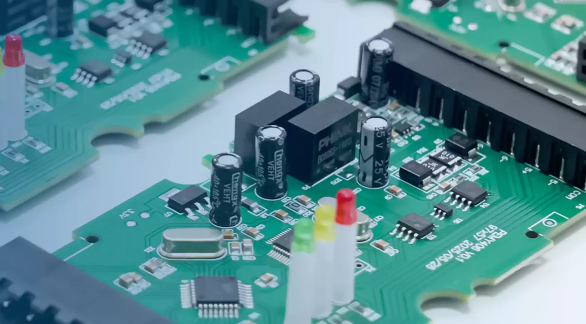
SMD Package Classification: From Chip Components to BGA Surface mount technology reshaped electronics by shrinking components to a fraction of their through-hole ancestors, and the packages that resulted are numerous enough to confuse anyone meeting them for the first time. Understanding how they are classified makes datasheets, assembly quotations and…
PCB Edge Plating: Design Rules, EMI Shielding and Thickness Edge plating is a feature that most boards never need and a few boards cannot work without. Instead of leaving the side wall of the laminate bare after routing, the fabricator deposits copper on it and connects that copper to the…
Military PCB versus Commercial PCB: Design and Reliability Ask whether a board is military or commercial and the answer rarely changes what the board does. It changes what the board is expected to survive. The same microcontroller, the same regulator and often the same laminate appear in both products, but…
Stackup Choices: Low Loss Laminate or FR4 Every board begins with a stackup, and that decision is hard to reverse. An FR4 PCB stackup fixes the dielectric constant, the loss, the layer count and the impedance targets before a single trace is routed, while a high frequency PCB stackup changes…
Sputtered versus Printed Conductors on a Ceramic PCB Ceramic substrates solve problems that FR4 cannot: they pull heat out of a device far faster, hold their dimensions at temperatures that would destroy an epoxy laminate, and lose very little energy at microwave frequencies. Once a design has settled on ceramic,…
Pad Design for Wave Soldering and Reflow A pad is not just a place to put solder. It is the shape that decides how much solder the joint receives, where that solder goes when it melts, and whether the part stays in place while the alloy is liquid. Two pads…
PCB Short Circuits: Tracing the Cause in Fabrication A short circuit found after fabrication is expensive, but the conditions that produce one are usually visible in the process long before the boards reach electrical test. Most shorts originate in the wet process, where a thin residue of metal survives the…
A PCB Design Process From Request to Release A PCB design process is less about the layout tool than about the sequence of checks that turn a schematic into a manufacturable board. Boards fail not because the routing was technically difficult but because the inputs were incomplete, the key nets…
Rigid Flex PCB Cost: Layer Count, Volume and Region Rigid flex boards are the most expensive mainstream interconnect technology in volume production, and they are also the one whose price is hardest to predict from a drawing alone. Layer count, flex layer material, stiffener placement, via structure and order quantity…
HDI Board vs Blind and Buried Via Boards Two boards can both be described as high density and still be built by completely different processes. One may need a single laser drilling step on each side of a conventional stack; the other may need two lamination cycles and four laser…