PCB Material Requirements: Copper Clad Laminate Selection Material selection is one of the few decisions on a circuit board that is difficult to reverse later. Changing the laminate after the design is released means changing impedance targets, thermal behaviour and often the fabrication process itself. Understanding what a copper clad…
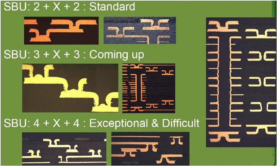
Test Coupon Requirements in PCB Production Portable electronics keep getting thinner and more capable at the same time, and the boards inside them have followed. High density interconnect construction has moved from a specialist technique into mainstream production, appearing in phones, tablets, package substrates and automotive navigation hardware. With that…
5G PCB Design Specification: Rules Before Layout A design specification exists to remove decisions from the layout engineer without removing judgement. It fixes the inputs, the setup and the constraints that apply to every board the same way, so that the interesting part of the work — the placement and…
How to Judge PCB Quality Before and After Assembly PCB quality is bought on price and judged afterwards, and the two are not unrelated. A supplier that quotes far below the market is usually reducing something, whether that is material grade, process time or inspection. Knowing what to examine, both…
Wave Soldering versus Reflow: Process Comparison Two processes form almost every solder joint in electronics. One deposits paste and heats the whole assembly in an oven, and the other brings the board across a standing wave of molten solder. They produce different joints, have different defect signatures and are often…
Rogers 4350B PCB: Properties, Stackup and Cost Guide Rogers 4350B has become the default laminate for a large share of RF, microwave and millimeter wave work, because it holds a stable dielectric constant, keeps loss low and still laminates like a conventional material. The catch is price: the raw sheet…
Megtron 6 PCB: Material Properties and Cost Drivers Megtron 6 sits in the top tier of high speed laminates, used where 25G, 56G and 112G channels have to cross a backplane or a switch card with enough margin left for the rest of the link budget. It achieves that with…
Laser Direct Imaging: Why Fine-Line Boards Depend On It Laser direct imaging has quietly become the technique that decides whether a fine-line design can be manufactured at all. Where a design calls for conductors and spaces measured in tens of microns, the traditional photographic process is at the edge of…
BGA Repair and Board-Level Fault Finding BGA repair on a board with a ball grid array package is less about the package than about the circuit around it. Most faults arrive as a symptom rather than as a diagnosis: a unit that sometimes starts, a supply that will not come…
High-Speed PCB Design Challenges: FPGAs, SSN and Routing It would be convenient if a high-speed PCB design could be laid out as easily as a schematic is drawn, but the two tasks draw on different knowledge. The schematic defines what the circuit does; the layout decides whether it does it…