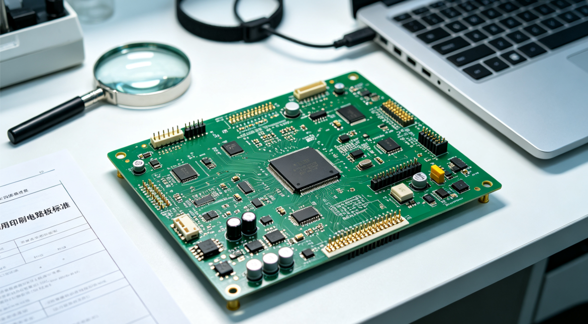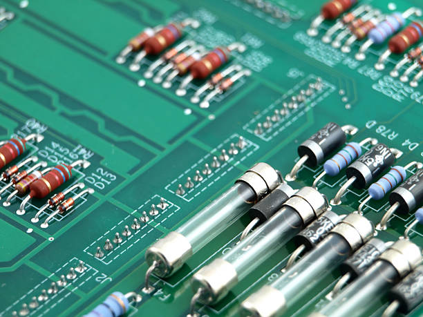
PCB Design: How to Reduce Errors and Improve Efficiency PCB design is a critical but time-consuming engineering task. Even a small design error can require engineers to inspect individual nets, components, and connections throughout an entire circuit. As PCB designs become more complex, maintaining accuracy and consistency becomes increasingly…
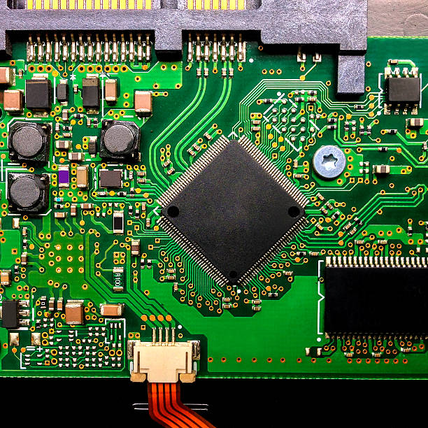
Essential PCB Design Basics Every Engineer Should Know A reliable printed circuit board starts with a solid understanding of fundamental design principles. PCB design is not simply about connecting components with traces. Layer stack-up, power distribution, grounding, signal return paths, component placement, routing, and manufacturing requirements must all work…
How to Solve EMI Problems in Multilayer PCB Design Electromagnetic interference (EMI) is a common challenge in high-speed and multilayer PCB design. EMI can originate from power distribution networks, high-speed signal transitions, poor return paths, excessive loop areas, and inappropriate layer stack-up. Modern EMI mitigation can involve shielding materials,…
14 Key Characteristics of a High-Reliability PCB At first glance, PCBs can look very similar regardless of their actual quality. However, differences in materials, manufacturing processes, dimensional control, surface treatment, and inspection can have a major impact on the board’s reliability throughout its service life. A PCB must maintain…
Best 6-Layer PCB Stackup for High-Speed Circuit Boards A six-layer PCB is widely used in embedded systems, industrial electronics, communication equipment, and other products that require a balance between routing density, signal integrity, power distribution, and manufacturing cost. For a High-Speed PCB, however, simply adding six copper layers does…
How to Output Gerber Files Correctly: A Complete Guide for PCB Engineers When a PCB design is completed, the design files must be converted into production-ready manufacturing data before the board can be fabricated. Among all manufacturing data formats, Gerber Files remain one of the most widely used formats…
How to Export PADS Gerber file: Complete PCB Guide Why Correct Gerber File Export Matters Gerber files are the primary manufacturing data used to convert a PCB design into physical circuit boards. Even when the PCB layout itself is correct, an incorrect or incomplete Gerber output can cause missing…
Multilayer PCB Impedance Routing Guidelines: Practical Differential Pair Design Tips Why Impedance Routing Matters in Multilayer PCB Design Smartphones, computers, high-definition displays, and other high-speed electronic devices all rely on PCBs to transmit increasingly large amounts of digital data. As signal speeds increase, maintaining controlled impedance becomes an essential…
Via-to-Trace Spacing in Multilayer PCB Design When designing a PCB, engineers focus heavily on how to connect signals between different layers efficiently and reliably. As signal density increases, especially in high-speed circuits, the number of vias used for interlayer connections also increases. The same discipline applies to Multilayer PCB Design,…
What Is a High-Reliability PCB? Reliability refers to the ability of a product to perform its specified function under specified conditions for a specified period of time. For electronic products, higher reliability means greater assurance that the product will continue to operate safely and consistently throughout its expected service…