Castellated: Design Rules and Process Limits
A castellated hole is a plated half hole on the edge of the board, and it exists so that a module can be soldered onto a carrier by its edge. The plating has to be continuous from the barrel through the cut face to the pad, which makes the process a combination of drilling, plating and routing rather than a single step.
What Edge Plating Is For
Modules and daughter boards that are soldered flat onto a mother board use castellations to make the connection along an edge. The alternative is a connector, and the castellation removes the connector from the bill of materials and from the height budget.
The joint is then a visible fillet on the edge rather than a hidden one, which helps inspection and puts the requirement on the plating rather than on a mating interface. Our plating thickness notes describe the barrel side of that requirement.
Process Sequence
The hole is drilled and plated as a full hole first, so that the barrel is formed with a complete cylinder. Only after plating is the edge routed through the centre of the hole, which turns it into a half cylinder with the plating exposed on the cut face.
The sequence matters because routing first leaves nothing to plate. It also means the castellation is created at the depanelling or the outline step, and the handling after that step has to protect an exposed edge. Our outline tolerance notes describe the routing side.
Plating Continuity on the Cut Face
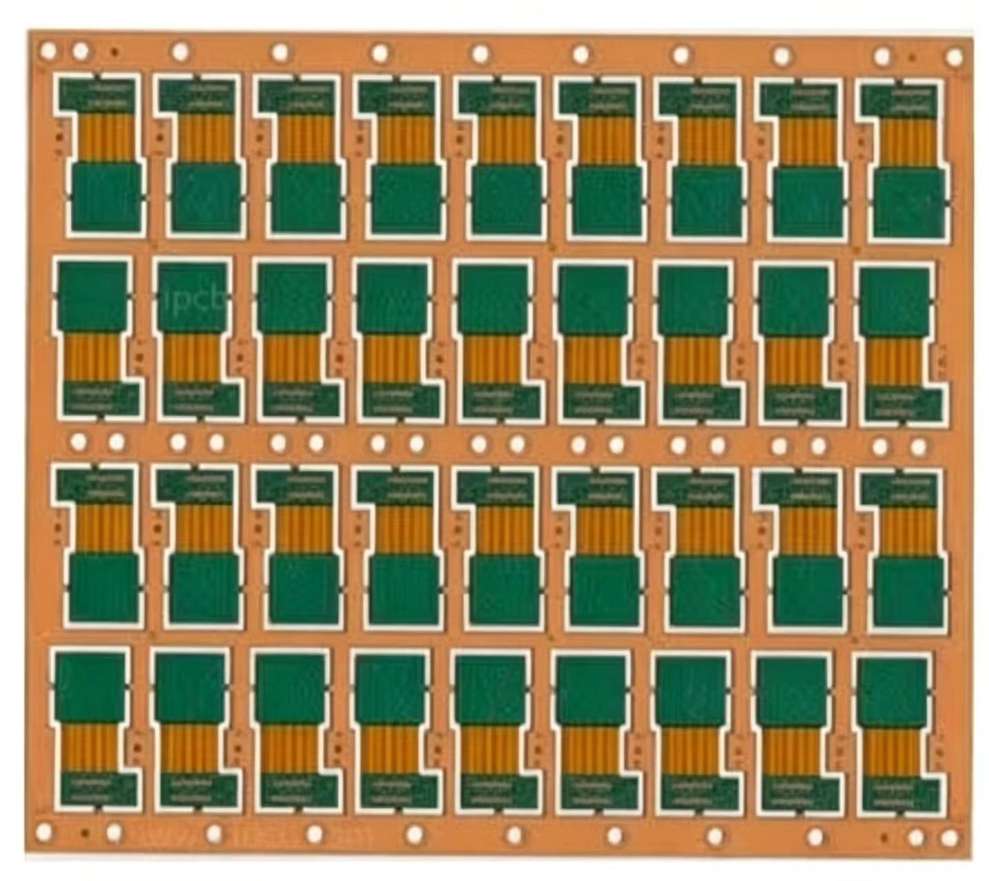
The routing exposes a copper section through the barrel wall, and the copper has to remain attached to the laminate along the whole cut. A cut that tears the plating or that lifts it from the wall leaves a castellation that looks correct and does not conduct reliably.
The risk is highest where the barrel plating is thin or where the laminate is brittle. That is the reason the plating thickness for a castellated design is specified above the general through hole requirement.

Design Rules for the Castellation
The castellation has a diameter, a pitch and a land on each side, and the pitch is usually set by the carrier footprint rather than by the module. The land on the module side has to be large enough to form a fillet after the cut, which means the pad is a partial annulus rather than a full one.
The remaining ring after the cut is what the solder wets, so a design that leaves a sliver of copper produces a joint that is thin at the edge. Our hole copper notes describe how the ring is controlled.
Solderability and the Exposed Copper
The cut face carries the surface finish that was applied before routing, and the finish on the exposed copper is what decides how the joint forms. A finish that oxidises quickly makes the module hard to solder after a short shelf life.
Where the module is stored before assembly, the finish selection is a balance between solderability and cost rather than a preference. The shelf life belongs in the specification alongside the finish.
Assembly Considerations
The module is placed on the carrier and soldered along the edge, and the joint is made by a fillet that wraps the castellation. Paste volume is set for the fillet rather than for a pad, so a stencil aperture that is sized from the pad alone will underfill.
Alignment is the second consideration, because the castellations have to line up with the carrier pads. A module that is offset by half a pitch produces a joint on one side of the edge and none on the other, and the defect is visible after reflow rather than before.
Inspection
Inspection is visual for the fillet along the edge and by cross section for the plating continuity through the cut. X-ray is of limited use on a castellation because the joint is on the outside surface.
The cross section is the check that proves the barrel is still attached to the laminate after the cut, which is the failure that a visual inspection cannot see. Our board quality notes describe how the sample is selected.
Process Control and Verification
The process window is set by the narrowest step in the flow, so an improvement anywhere else shows up as margin rather than as yield until that step is addressed. A short note on the drawing about handling, storage or packaging is often worth more than an extra decimal place on a tolerance.
Where a value sits close to a process limit, the drawing should say so, since the shop can then open the process window rather than working to a nominal figure that carries no tolerance. A stack-up that is drawn rather than described removes most of the ambiguity from a quotation, and it lets the fabricator price the board against the dielectric and copper weights that will actually be used.
Checks Before Release
The checks that matter are the ones performed on the product rather than on a sample kept for the purpose, because a coupon that travels with the panel is the only evidence about that panel. Where a requirement can be measured, it should be measured at the point of manufacture and recorded against the board or the lot it applies to.
A parameter that is set once and never re verified drifts, and the drift is usually discovered by a defect rather than by the record.
FAQ
Can a castellation be added after the board is routed? No. The barrel has to be plated before the edge is cut through it, so the sequence is fixed at the design stage.
Are castellations suitable for a high current connection? They can be, and the current is limited by the cross section of the remaining plating rather than by the pad area.
What does gopcb provide for edge plating? We provide castellation design with the remaining ring and the pitch defined, plating thickness specified above the general requirement, a sequence that plates before routing, finish and shelf life matched to the assembly plan, and cross sections that prove continuity after the cut.