High Layer Count PCB Manufacturing: 20+ Layer PCB Process
As the electronics industry continues to evolve toward higher density, greater reliability, and more compact designs, High Layer Count PCB technology has become an important foundation for advanced electronic equipment. Compared with conventional multilayer boards, PCBs with more than 20 layers require significantly higher levels of manufacturing precision, process coordination, and quality control.
The manufacturing of a 20 Layer PCB is not simply a matter of increasing the number of copper layers. It is a complex process involving material selection, multilayer stacking, lamination, drilling, plating, circuit formation, surface finishing, and inspection. Each stage must be carefully controlled to ensure stable electrical performance and mechanical reliability.
For demanding electronic applications, reliable Multilayer PCB Manufacturing plays an important role in determining the overall performance and long-term reliability of the finished product.
Material Selection and Pre-Treatment for High Layer Count PCBs
The manufacturing process starts with careful material selection and pre-treatment. A High Layer Count PCB with more than 20 layers requires materials with excellent dimensional stability and process compatibility.
The selected substrate must withstand repeated high-temperature and high-pressure processing without excessive deformation or delamination. Material stability is particularly important because dimensional changes can accumulate across multiple layers and affect the final layer registration.
Before lamination, the material surface is carefully prepared to remove contaminants, oxidation, and other unwanted residues. Controlled surface roughening can also improve interlayer bonding and provide a stronger foundation for subsequent processing.
Material consistency should be maintained throughout production. Variations in substrate properties, thickness, or other material characteristics can influence the performance and reliability of a 20 Layer PCB.
PCB Lamination for 20+ Layer Structures
PCB Lamination is one of the most critical processes in high layer count PCB manufacturing. A board with more than 20 layers typically requires multiple lamination cycles to combine inner-layer cores and bonding materials into a stable multilayer structure.
During lamination, the individual layers are carefully stacked and subjected to controlled temperature and pressure. The objective is to achieve strong and uniform bonding between the layers while maintaining accurate layer registration.
Precise control of the lamination process helps prevent common defects such as:
- Voids
- Excessive resin flow
- Delamination
- Uneven bonding
- Layer misalignment
For a complex 20 Layer PCB, even a small variation in temperature, pressure, or alignment can affect subsequent drilling, routing, and interlayer connections. Therefore, stable PCB Lamination parameters are essential for consistent production quality.
PCB Drilling and Plating for Interlayer Connections
Drilling and plating create the electrical pathways that connect different layers within a multilayer board. As the layer count increases, the internal structure becomes more complex, making drilling accuracy increasingly important.
During the drilling process, holes must be positioned accurately and formed through the required layers without damaging internal circuitry. Proper drilling also helps ensure smooth and complete hole walls for subsequent metallization.
After drilling, the hole walls are prepared for copper deposition. Copper plating creates a conductive layer inside the holes and across the required circuit surfaces, establishing reliable electrical connections between different layers.
For complex Multilayer PCB Manufacturing, drilling and plating must be carefully coordinated with the board stack-up and interconnection requirements. Inadequate hole quality or uneven copper deposition can negatively affect electrical continuity and long-term reliability.
GOPCBA’s manufacturing capabilities include mechanical and laser drilling as well as PTH copper plating for advanced PCB fabrication.
Circuit Formation and Surface Finishing
Circuit formation and surface finishing are important stages in producing the final PCB structure.
During circuit formation, controlled etching removes unwanted copper and creates the required trace pattern. The process must maintain accurate line geometry while preventing defects such as open circuits, short circuits, and excessive dimensional variation.
For a high layer count board, circuit accuracy becomes particularly important because the available routing space can be limited and the internal structure is highly interconnected.
Surface finishing is then applied to protect exposed copper surfaces and improve the board’s suitability for component assembly. Depending on the application, the appropriate finish can improve corrosion resistance, wear resistance, and solderability.
These processes form an important part of the overall Multilayer PCB Manufacturing workflow and must remain consistent with the electrical, mechanical, and assembly requirements of the final application.
Quality Inspection Throughout PCB Manufacturing
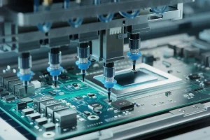
A comprehensive PCB Quality Control system is essential for high layer count boards. Because a 20+ layer PCB contains a large number of interconnected structures, a small manufacturing defect can potentially affect the operation of the complete electronic system.
Inspection should therefore be integrated into multiple stages of production rather than being limited to final inspection.
Key inspection areas can include:
- Layer alignment
- Lamination quality
- Hole-wall condition
- Drilling accuracy
- Copper plating uniformity
- Circuit geometry
- Surface finish quality
- Electrical continuity
Advanced inspection technologies can help identify defects such as internal delamination, hole-wall abnormalities, and circuit deviations.
GOPCBA’s published quality management information describes quality control across PCB design review, DFM checking, PCB manufacturing, testing, incoming materials, and production processes. Its PCB manufacturing process also includes AOI, X-ray inspection, electrical testing, and final inspection.
Electrical Testing and Final Verification
Electrical testing provides an additional level of verification before the finished PCB is delivered.
For complex multilayer boards, testing can help verify circuit continuity, insulation performance, and electrical integrity. This is particularly important when the board contains a large number of internal connections and complex routing structures.
A reliable manufacturing workflow combines process inspection with electrical verification to reduce the possibility of defective boards reaching the next stage of production or final assembly.
For applications requiring additional verification after component assembly, PCB Quality Control can be complemented by dedicated PCB assembly and testing processes.
GOPCBA provides PCB and PCBA testing services designed to verify electrical performance and product functionality according to application and customer requirements.
Multi-Process Coordination in High Layer Count PCB Manufacturing
The manufacturing capability of a High Layer Count PCB is determined not by a single production step, but by the coordination of the entire manufacturing workflow.
From material preparation and PCB Lamination to drilling, copper plating, circuit formation, surface finishing, and final inspection, each process affects the next. A deviation introduced during one stage may create problems during subsequent manufacturing steps.
For this reason, high layer count PCB production requires:
- Stable manufacturing parameters
- Accurate process control
- Appropriate production equipment
- Consistent raw materials
- Experienced engineering support
- Comprehensive inspection procedures
Effective coordination is particularly important for a 20 Layer PCB and other high layer count structures because dimensional tolerances and registration requirements become increasingly demanding as the number of layers increases.
Applications of 20+ Layer PCBs
High layer count PCBs are commonly associated with advanced electronic systems that require high routing density, complex power distribution, multiple signal layers, and reliable interlayer connections.
Typical applications include:
5G Communication Equipment
Advanced communication systems require compact boards with high routing density and reliable signal transmission. High layer count structures can provide additional routing and power distribution resources within a limited board area.
Servers and AI Computing Systems
Servers and AI computing hardware often contain high-speed interfaces, complex power systems, and large numbers of electronic components. Multilayer structures help accommodate these complex electrical requirements.
Medical Electronics
Medical equipment requires reliable electronic systems with stable performance and high manufacturing consistency. High layer count PCBs can support complex circuit architectures within compact equipment.
Industrial Control Systems
Industrial control equipment may require multiple power, control, communication, and signal circuits on a single board. High layer count PCB structures provide the routing density required for these applications.
Aerospace and Advanced Electronics
Aerospace and other demanding applications place strong requirements on reliability, dimensional stability, and electrical performance. Carefully controlled Multilayer PCB Manufacturing can help support these requirements.
The Importance of Advanced High Layer Count PCB Manufacturing
As electronic products become smaller, faster, and more integrated, PCB structures are becoming increasingly complex. Higher layer counts provide designers with additional routing layers, power planes, ground structures, and interconnection options.
However, increasing the number of layers also increases manufacturing complexity. Precise material selection, stable PCB Lamination, accurate drilling and plating, controlled circuit formation, and comprehensive PCB Quality Control must work together to achieve consistent results.
For advanced electronic applications, the ability to manufacture a reliable High Layer Count PCB is therefore an important part of modern electronics manufacturing.
Conclusion
Manufacturing a 20 Layer PCB or other 20+ layer structure requires a coordinated and highly controlled production process. From material selection and pre-treatment to PCB Lamination, drilling, copper plating, circuit formation, surface finishing, and final testing, every stage contributes to the reliability of the finished board.
As demand continues to grow for 5G communication systems, servers, AI hardware, medical equipment, industrial controls, and aerospace electronics, advanced Multilayer PCB Manufacturing will continue to play an important role in supporting increasingly complex electronic designs.
A combination of precise manufacturing processes, stable materials, accurate interlayer connections, and comprehensive PCB Quality Control provides the foundation for producing reliable high layer count PCBs for demanding applications.