Reflow Soldering for PCB Assembly: Process, Temperature Profile, Defects, and Best Practices
Reflow soldering is one of the most important processes used in modern PCB assembly and surface-mount technology (SMT) production. It is primarily used to attach surface-mount devices (SMDs) to a printed circuit board (PCB) by melting solder paste under carefully controlled temperature conditions.
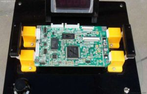
The basic process involves applying solder paste to the designated pads on a PCB, accurately placing electronic components on the solder deposits, and then passing the assembled board through a reflow soldering oven. The controlled heating process melts the solder paste, allowing it to wet the component terminals and PCB pads. When the assembly cools, the molten solder solidifies and forms strong mechanical and electrical connections.
As electronic products become smaller, lighter, faster, and more functionally complex, manufacturers increasingly rely on high-density SMT assembly. From tiny 0201 passive components to advanced ball grid array (BGA), QFN, and other fine-pitch packages, reflow soldering provides the precision, repeatability, and production efficiency required for modern PCB assembly.
The quality of reflow soldering has a direct impact on the electrical performance, mechanical reliability, service life, and overall quality of an electronic product. Therefore, controlling solder paste printing, component placement, thermal profiles, and inspection processes is essential for producing reliable PCBs.
This guide explains the PCB reflow soldering process, how a reflow oven works, the different temperature zones, common reflow profiles, soldering techniques, common defects, lead-free reflow considerations, and best practices for reliable PCB assembly.
What Is Reflow Soldering in PCB Assembly?
Reflow soldering is a thermal soldering process used primarily for attaching surface-mount components to a PCB.
Unlike traditional hand soldering, reflow soldering does not require each component terminal to be soldered individually. Instead, solder paste is first deposited onto multiple PCB pads. Components are then positioned on these deposits, and the entire assembly is heated according to a predefined temperature profile.
The solder paste normally contains fine solder alloy particles and flux. During heating, the flux becomes active and helps remove surface oxides. As the temperature rises above the solder alloy’s melting point, the solder particles melt and form a continuous solder joint between the component terminals and PCB pads.
After the board passes through the cooling zone, the solder solidifies and creates a permanent connection.
A typical reflow soldering process includes:
- PCB preparation
- Solder paste printing
- Component placement
- Solder paste inspection
- Reflow soldering
- Post-reflow inspection and testing
The process is highly suitable for automated SMT PCB assembly, especially for high-volume production and electronic products containing a large number of surface-mount components.
How Does a Reflow Soldering Oven Work?
A reflow soldering oven is a specialized piece of equipment designed to heat an assembled PCB according to a controlled thermal profile.
Modern reflow ovens typically contain multiple independently controlled heating and cooling zones. Each zone operates within a specific temperature range and performs a particular function during the soldering process.
The board gradually moves through these zones on a conveyor. Instead of applying heat suddenly, the oven gradually increases and controls the temperature of the PCB assembly.
The main objectives are to:
- Prevent thermal shock to the PCB and components
- Activate the solder paste flux
- Bring the entire assembly to the required soldering temperature
- Melt the solder alloy completely
- Promote proper solder wetting
- Control cooling and solder solidification
- Minimize soldering defects
The number of zones varies according to the oven design and production requirements. High-end production equipment can provide highly precise thermal control, making it possible to develop customized profiles for different PCB assemblies and component configurations.
Step-by-Step PCB Reflow Soldering Process
A reliable PCB reflow soldering process depends on controlling every stage before, during, and after heating.
1. PCB Preparation and Surface Cleaning
Before solder paste printing, the PCB should be properly prepared and free from contaminants that could affect solderability.
Dust, oil, moisture, oxidation, and other contaminants can interfere with solder wetting and may contribute to defects such as insufficient soldering, open circuits, or poor adhesion.
Depending on the application, PCB cleaning may include:
- Ultrasonic cleaning
- Water-based cleaning
- Solvent cleaning
- Specialized PCB cleaning systems
However, not every SMT assembly requires post-fabrication cleaning. The appropriate cleaning strategy depends on the PCB surface finish, solder paste, flux chemistry, product requirements, and assembly process.
Proper material storage and handling are equally important. Moisture-sensitive components and PCB materials should be stored and handled according to their applicable requirements.
2. Solder Paste Printing
Solder paste printing is a critical stage in PCB assembly because the volume and location of solder paste directly influence final solder joint quality.
A stainless-steel stencil is positioned over the PCB. A squeegee then pushes solder paste through precisely designed apertures onto the PCB pads.
The stencil must be designed according to the PCB layout, component package, pad geometry, and required solder volume.
Important parameters include:
- Stencil thickness
- Aperture dimensions
- Aperture-to-pad ratio
- Squeegee pressure
- Printing speed
- Separation speed
- PCB and stencil alignment
- Solder paste condition
An optimized stencil design can significantly reduce solder bridging, insufficient solder, solder balling, and other defects.
3. Component Placement
After solder paste printing, components are accurately placed onto the PCB using an automated pick-and-place machine.
The machine identifies component locations from the PCB design data and positions each component according to the required coordinates and orientation.
Placement accuracy is especially important for high-density PCB assemblies containing:
- 0201 and 01005 passive components
- Fine-pitch ICs
- QFN packages
- BGA packages
- CSP packages
- High-pin-count components
Incorrect placement can lead to component misalignment, tombstoning, solder bridging, insufficient solder contact, or open circuits.
For high-volume manufacturing, automated optical alignment and machine calibration help maintain consistent placement accuracy.
4. Solder Paste Inspection and Pre-Reflow Inspection
Before the PCB enters the reflow oven, manufacturers commonly perform inspection to verify the quality of solder paste printing and component placement.
Solder Paste Inspection (SPI) systems measure characteristics such as:
- Solder paste volume
- Paste height
- Deposit area
- Position accuracy
- Shape and coverage
SPI helps identify printing problems before the board reaches the reflow stage.
Pre-reflow inspection can prevent defects from progressing to later manufacturing stages and can reduce material waste and rework costs.
5. Reflow Soldering
After inspection, the populated PCB enters the reflow oven.
The board moves through a sequence of controlled temperature zones. The heating profile must be carefully selected according to the solder paste manufacturer’s specifications, PCB structure, component limitations, and assembly requirements.
The four fundamental stages are generally:
Preheating Zone
During preheating, the PCB temperature gradually increases.
The purpose is to:
- Reduce thermal shock
- Evaporate volatile materials
- Begin flux activation
- Prepare the assembly for the next stage
An excessively rapid temperature increase may damage sensitive components or cause solder paste-related defects.
Soak Zone
In the soak zone, the PCB remains within a controlled temperature range for a specified period.
This stage helps:
- Activate the flux
- Equalize temperature differences across the PCB
- Prepare the solder paste for melting
- Reduce thermal gradients between large and small components
Temperature uniformity is particularly important for complex or high-density PCBs.
Reflow Zone
The reflow zone is where the solder alloy reaches its melting temperature.
Once the solder becomes molten, it wets the PCB pads and component terminals, creating the solder joints required for electrical and mechanical connection.
The peak temperature and time above liquidus must be carefully controlled.
Too little heat may result in incomplete solder melting or poor wetting, while excessive heat may damage components, PCB materials, or solder joints.
Cooling Zone
After reflow, the PCB enters the cooling zone.
The molten solder gradually solidifies, creating the final solder joints.
Controlled cooling helps establish appropriate solder joint structure and minimizes excessive thermal stress.
Reflow Soldering Temperature Profile
The reflow soldering temperature profile describes how PCB temperature changes as the board travels through the reflow oven.
An appropriate profile is essential for achieving consistent soldering quality. The exact profile should not be selected solely from generic temperature values. Instead, it should be developed according to the solder paste manufacturer’s recommendations and the thermal characteristics of the actual PCB assembly.
Important parameters include:
- Ramp rate
- Soak temperature and duration
- Time above liquidus (TAL)
- Peak temperature
- Cooling rate
- Temperature difference across the PCB
Common profile approaches include:
Ramp-Soak-Spike (RSS)
The temperature gradually rises during the initial ramp, enters a soak period, and then increases toward the required peak reflow temperature.
This profile can help manage thermal differences across complex assemblies.
Ramp-to-Spike (RTS)
The temperature increases continuously toward the peak temperature without a prolonged soak stage.
RTS profiles can be suitable for certain solder pastes and PCB assemblies when the process window permits.
Customized Reflow Profile
For complex PCB assemblies, manufacturers may develop customized thermal profiles according to:
- PCB thickness
- Copper distribution
- Number of PCB layers
- Component density
- Component thermal sensitivity
- Solder paste specifications
- Surface finish
- Assembly requirements
Thermal profiling should be periodically verified, especially when changing PCB designs, solder paste materials, component mixes, or production conditions.
Common Reflow Soldering Technologies
Different heating technologies can be used for PCB assembly, depending on production requirements.
Convection Reflow Soldering
Convection reflow uses heated air or gas to transfer thermal energy to the PCB assembly.
It is one of the most widely used methods because it provides relatively uniform heating and precise process control.
Advantages include:
- Good temperature uniformity
- Suitable for complex PCB assemblies
- Strong process repeatability
- Compatibility with lead-free soldering
- High production efficiency
Infrared Reflow Soldering
Infrared reflow uses infrared radiation to heat the PCB and components.
It can provide rapid heating but may have limitations related to component size, material properties, shadowing effects, and temperature uniformity.
Vapor Phase Reflow
Vapor phase reflow uses the heat released during condensation of a specialized vapor to heat the PCB.
Because the process can provide highly controlled heat transfer and a relatively uniform temperature environment, vapor phase technology can be useful for specialized and temperature-sensitive assemblies.
Nitrogen Reflow Soldering
Nitrogen reflow creates a low-oxygen atmosphere inside the reflow oven.
Reducing oxygen exposure can help minimize oxidation during soldering and may improve solder wetting and solder joint appearance, particularly for certain applications and solder materials.
The need for nitrogen depends on the solder paste, product requirements, process window, and cost considerations.
Best Practices for Reliable PCB Reflow Soldering
Achieving reliable solder joints requires more than simply selecting a high-quality reflow oven. The entire PCB assembly process must be controlled.
Optimize Stencil Design
Stencil design should be matched to PCB pad geometry and component packages.
For fine-pitch and miniature components, optimized aperture dimensions and appropriate stencil thickness can help control solder volume and reduce bridging.
Stencil design should be evaluated using applicable industry guidance, including IPC recommendations where appropriate.
Control the Reflow Temperature Profile
The thermal profile should be measured and validated rather than assumed.
Manufacturers should regularly verify:
- Peak temperature
- Ramp rate
- Soak time
- Time above liquidus
- Cooling rate
- Temperature uniformity
Maintain Accurate Component Placement
Pick-and-place machines should be regularly calibrated and maintained.
Accurate placement is particularly important for fine-pitch components, BGA packages, QFN devices, and miniature passive components.
Use High-Quality Solder Paste
Solder paste quality has a direct influence on printing performance and solder joint reliability.
Manufacturers should control:
- Storage temperature
- Shelf life
- Handling conditions
- Stencil printing time
- Paste viscosity
- Moisture exposure
Control PCB and Component Moisture
Moisture can become a serious concern during high-temperature soldering.
Moisture-sensitive components should be handled according to their applicable moisture sensitivity requirements. Proper storage and floor-life management can reduce the risk of package cracking and other moisture-related failures.
Implement Process Inspection
SPI, AOI, X-ray inspection, and electrical testing can be combined to identify defects at different stages of the PCB assembly process.
A strong inspection strategy allows manufacturers to identify process trends early rather than relying only on final inspection.
Common PCB Reflow Soldering Defects and How to Prevent Them
Even a highly automated PCB assembly line can experience soldering defects if process parameters are not properly controlled.
Common defects include the following.
Tombstoning
Tombstoning, also known as the Manhattan effect, occurs when one end of a small passive component lifts away from the PCB pad during reflow.
Common causes include:
- Uneven solder paste deposits
- Uneven heating
- Pad design imbalance
- Component misalignment
- Different thermal characteristics between the two pads
Preventive measures include optimizing stencil apertures, improving pad design, balancing thermal conditions, and ensuring accurate component placement.
Cold Solder Joints
A cold solder joint occurs when the solder does not form an adequate metallurgical connection.
Potential causes include:
- Insufficient temperature
- Insufficient time above liquidus
- Poor solder wetting
- Oxidation
- Contaminated surfaces
Optimizing the thermal profile and maintaining clean solderable surfaces can reduce this problem.
Solder Bridging
Solder bridging occurs when molten solder connects two adjacent pads or terminals, potentially causing an electrical short circuit.
Common causes include:
- Excessive solder paste
- Poor stencil design
- Incorrect component placement
- Excessive solder paste spread
- Fine-pitch printing problems
Solutions include optimizing stencil apertures, controlling solder paste volume, improving placement accuracy, and maintaining proper printing parameters.
Solder Balls
Solder balls are small spherical particles of solder that may appear around solder joints after reflow.
Possible causes include:
- Improper solder paste storage
- Excessive heating rate
- Excessive solder paste volume
- Moisture
- Inappropriate reflow profile
Proper solder paste handling, stencil optimization, and thermal profile control can reduce solder ball formation.
Insufficient Solder
Insufficient solder occurs when the solder joint does not contain enough solder to create the required connection.
Potential causes include:
- Insufficient solder paste deposition
- Blocked stencil apertures
- Poor printing parameters
- Incorrect stencil design
- Poor PCB surface condition
SPI can be used to identify insufficient solder paste before the PCB enters the reflow oven.
Lead-Free Reflow Soldering for High-Density PCB Assembly
Environmental regulations and industry requirements have accelerated the adoption of lead-free soldering processes.
Lead-free solder alloys generally require higher processing temperatures than traditional tin-lead solder systems. As a result, lead-free PCB assembly requires careful thermal management.
Important considerations include:
- Higher peak temperatures
- Accurate thermal profiling
- Component temperature limitations
- PCB material selection
- Flux activity
- Solder paste selection
- Oven temperature uniformity
High-density interconnect (HDI) PCBs create additional challenges because their compact structures often contain fine lines, microvias, small pads, and closely spaced components.
As component sizes decrease and PCB density increases, thermal distribution becomes more difficult to manage. Large copper areas may absorb more heat, while small components can reach target temperatures more quickly.
Therefore, the reflow profile should be validated using actual production boards whenever possible.
Reflow Soldering vs. Wave Soldering for PCB Assembly
Reflow soldering and wave soldering are both widely used PCB assembly technologies, but they are designed for different component types and applications.
| Factor | Reflow Soldering | Wave Soldering |
|---|---|---|
| Primary application | Surface-mount components | Through-hole components |
| Solder material | Solder paste | Molten solder |
| Main process | Solder paste + controlled heating | PCB passes over a molten solder wave |
| SMT compatibility | Excellent | Limited, although selective applications are possible |
| THT compatibility | Limited | Excellent |
| Automation | Highly automated | Highly automated |
| Typical applications | Dense SMT PCB assemblies | Through-hole and mixed-technology assemblies |
| Process control | Precise thermal profile | Controlled solder wave and conveyor parameters |
For modern high-density SMT PCB assembly, reflow soldering is generally the primary soldering method. Wave soldering or selective soldering may be added when a PCB contains through-hole components.
Applications of Reflow Soldering in Electronics Manufacturing
As electronic devices continue to become smaller and more powerful, reflow soldering has become essential to modern electronics manufacturing.
Common applications include:
Consumer Electronics
Smartphones, tablets, laptops, wearables, smart home products, and other compact electronic devices rely heavily on high-density SMT assembly.
Automotive Electronics
Automotive control modules, infotainment systems, sensors, battery management systems, lighting systems, and other automotive electronics require highly reliable PCB assembly processes.
Industrial Electronics
Industrial controllers, automation equipment, power management systems, instrumentation, and communication equipment commonly use SMT and reflow soldering.
Medical Electronics
Medical monitoring equipment, diagnostic systems, portable medical devices, and other electronic products require reliable solder joints and tightly controlled manufacturing processes.
Telecommunications
Networking equipment, wireless communication devices, routers, switches, and other high-speed electronics depend on reliable high-density PCB assemblies.
Aerospace and Defense Electronics
Mission-critical electronics require strict process control, traceability, inspection, and reliability. Reflow soldering is an important part of the manufacturing process for many advanced aerospace and defense PCB assemblies.
How to Choose a Reliable PCB Assembly Partner for Reflow Soldering
Choosing the right manufacturing partner is an important decision when outsourcing PCB assembly.
A capable supplier should have the equipment, engineering expertise, process controls, and quality management systems necessary to handle the required PCB complexity.
When evaluating a PCB assembly manufacturer, consider the following factors:
Advanced Reflow Equipment
The manufacturer should have modern reflow ovens capable of providing stable and repeatable thermal profiles.
SPI, AOI, and X-Ray Inspection
A comprehensive inspection system helps identify solder paste, placement, and hidden solder joint defects.
For BGA and other bottom-terminated components, X-ray inspection can provide valuable information that cannot be obtained through conventional optical inspection.
Experience with High-Density PCBs
The manufacturer should have experience working with:
- Fine-pitch SMT
- BGA
- QFN
- HDI PCB
- Mixed-technology PCB assembly
- Lead-free assembly
- High-layer-count PCB
- Complex thermal designs
Strong Process Control
Reliable PCB assembly requires controlled processes rather than relying only on final inspection.
A professional manufacturer should maintain documented procedures for solder paste handling, stencil printing, component placement, reflow profiling, inspection, testing, and traceability.
Quality Management
Relevant quality systems and industry standards can provide additional confidence in manufacturing consistency.
Depending on the application, customers may consider certifications and standards such as ISO 9001, IPC-A-610, IATF 16949, ISO 13485, AS9100, and other applicable requirements.
Kingda: Reliable PCB Manufacturing and Assembly Solutions
Kingda provides professional PCB manufacturing and PCB assembly services for customers requiring reliable, high-quality electronic assemblies.
With integrated manufacturing capabilities, advanced production equipment, and strict quality control, Kingda supports PCB projects ranging from prototypes and small-batch production to high-volume manufacturing.
Our capabilities can support different PCB technologies and assembly requirements, including:
- Rigid PCB
- Multilayer PCB
- HDI PCB
- Flexible PCB
- Rigid-flex PCB
- High-density SMT assembly
- BGA assembly
- Lead-free PCB assembly
- Mixed SMT and through-hole assembly
For demanding applications, process control is applied throughout solder paste printing, component placement, reflow soldering, inspection, and final testing.
By combining engineering support, manufacturing capabilities, and quality control, Kingda helps customers reduce production risks, improve assembly consistency, and achieve reliable electronic products.
Conclusion: Why Reflow Soldering Matters for PCB Assembly
Reflow soldering is a fundamental technology in modern PCB assembly, particularly for surface-mount components and high-density electronic products. By combining controlled solder paste printing, precise component placement, accurate thermal profiling, and comprehensive inspection, manufacturers can produce consistent and reliable solder joints.
The reflow soldering temperature profile is one of the most important factors affecting solder quality. Preheating, soaking, reflow, and cooling must be carefully controlled to achieve proper solder melting, wetting, and solidification without exceeding component or PCB material limitations.
As electronic products become increasingly compact and sophisticated, challenges such as fine-pitch components, BGA packages, HDI structures, lead-free soldering, and complex thermal distributions require more advanced process control.
Therefore, selecting an experienced PCB assembly manufacturer is essential. A capable partner should provide modern reflow equipment, SPI, AOI, X-ray inspection, accurate component placement, thermal profiling, strong process management, and appropriate quality systems.
With the right equipment, materials, engineering expertise, and manufacturing controls, reflow soldering can provide the reliable solder joints required for high-performance electronic products.
For customers seeking dependable PCB manufacturing and assembly solutions, Kingda can provide integrated support from PCB fabrication and component assembly through inspection and testing, helping transform PCB designs into reliable finished electronic assemblies.