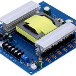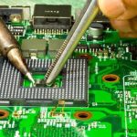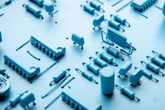
Lead-Free PCB Assembly has become a widely adopted manufacturing approach as electronics manufacturers respond to environmental regulations, customer requirements, and the growing demand for more sustainable production. In a typical PCB Assembly process, electronic components are soldered to a printed circuit board using technologies such as surface mount technology (SMT), through-hole assembly, wave soldering, selective soldering, or manual soldering.
The primary difference between leaded and lead-free assembly is the composition of the solder alloy. Traditional leaded solder commonly contains tin and lead, while lead-free solder uses alternative alloy systems, such as tin-silver-copper (SAC) or tin-copper (Sn-Cu).
For manufacturers, switching to Lead-Free Solder is not simply a matter of replacing one solder alloy with another. The soldering temperature, PCB materials, component temperature ratings, flux selection, equipment settings, thermal profiles, and inspection procedures may all need to be considered.
What Is Lead-Free PCB Assembly?
Lead-Free PCB Assembly refers to the assembly of electronic components onto a PCB using solder materials that meet the applicable lead-content requirements of environmental regulations and customer specifications.
In many commercial electronics applications, lead-free assembly is associated with RoHS PCB Assembly, because RoHS restricts the concentration of lead and other hazardous substances in covered products and materials. However, “RoHS-compliant” and “lead-free” should not automatically be treated as identical terms. Compliance depends on the complete product, applicable exemptions, material declarations, and the specific regulatory requirements involved.
Lead-free assembly can be performed using several manufacturing processes, including:
- SMT Assembly with lead-free solder paste
- Through-hole soldering
- Wave soldering
- Selective soldering
- Manual soldering and rework
- Reflow soldering for surface-mounted components
Leaded Solder vs. Lead-Free Solder
Historically, tin-lead solder alloys such as Sn63/Pb37 and Sn60/Pb40 were widely used because of their favorable melting characteristics, good wetting performance, and established manufacturing processes.
Today, lead-free solder alloys are widely used in electronics manufacturing. SAC305 is one of the commonly used lead-free alloys for SMT applications and typically consists of approximately 96.5% tin, 3.0% silver, and 0.5% copper.
Other lead-free alloys are also available, including tin-copper, tin-silver, and low-temperature solder systems. The appropriate alloy depends on the PCB design, component requirements, soldering process, reliability requirements, and customer specifications.
Common examples include:
| Solder Type | Typical Alloy | Typical Application |
|---|---|---|
| Leaded solder | Sn63/Pb37 | Applications where leaded solder is permitted |
| Lead-free solder | SAC305 | SMT reflow and general electronics assembly |
| Lead-free solder | Sn-Cu alloys | Wave and selective soldering |
| Low-temperature lead-free solder | Various Sn-based alloys | Temperature-sensitive applications |
The exact alloy composition should always be confirmed with the solder-material supplier and the customer’s manufacturing specification.
Why Is Lead-Free PCB Assembly Used?
The adoption of Lead-Free PCB Assembly is driven by several factors.
Environmental and Regulatory Requirements
Lead is a restricted substance in many electronics regulations. For products intended for regulated markets, manufacturers need to evaluate applicable requirements and determine whether lead restrictions apply to the product.
This is one of the main reasons RoHS PCB Assembly has become common in commercial electronics manufacturing.
Customer Requirements
Even when a particular market does not legally require a lead-free process, customers may specify lead-free materials as part of their product, environmental, or supply-chain requirements.
Product Lifecycle Considerations
Using a standardized lead-free manufacturing process can simplify production when products are intended for multiple markets with different regulatory requirements. However, the applicable regulations and exemptions should always be reviewed for the specific product.
When Should Lead-Free PCB Assembly Be Used?
The appropriate soldering process depends on the product, target market, components, PCB materials, and applicable regulations.
Lead-free assembly may be particularly appropriate when:
- The product must meet applicable RoHS requirements.
- Customers specifically require lead-free materials.
- The product is intended for markets where lead restrictions apply.
- The manufacturer wants to establish a lead-free production process.
- Environmental material requirements are included in the product specification.
- The components and PCB materials are compatible with the required lead-free soldering temperatures.
Lead-free assembly is not simply a marketing preference. It should be evaluated as part of the overall product compliance and manufacturing strategy.
Key Differences Between Leaded and Lead-Free PCB Assembly
1. Solder Alloy Composition
The most obvious difference is the solder alloy.
Traditional Sn63/Pb37 solder contains approximately 63% tin and 37% lead. SAC305 contains approximately 96.5% tin, 3% silver, and 0.5% copper.
The alloy composition directly affects melting behavior, wetting characteristics, mechanical properties, processing temperature, and cost.
2. Melting Temperature
Lead-free and leaded solder generally have different melting characteristics.
Sn63/Pb37 solder has a melting point of approximately 183°C. SAC305 has a melting range around 217–220°C.
Because lead-free alloys generally require higher soldering temperatures, the PCB Manufacturing process may require adjustments to reflow profiles, wave-soldering parameters, component selection, and thermal management.
The actual peak temperature and time-above-liquidus should not be selected from a generic value alone. The solder-paste manufacturer’s profile recommendations, component specifications, PCB material system, and assembly requirements should be considered together.
3. Process Window
Leaded solder has a long-established process history and generally offers a familiar process window. Lead-free solder can require tighter control of solder paste printing, thermal profiling, oxidation, wetting, and component compatibility.
This makes process control particularly important for high-reliability applications.
4. Material and Process Cost
Lead-free solder alloys may have higher material costs, particularly when silver-containing alloys such as SAC305 are used.
However, total assembly cost depends on much more than solder price. It can also include:
- PCB material selection
- Component compatibility
- Reflow or wave-soldering energy consumption
- Equipment requirements
- Process development
- Inspection
- Rework
- Yield
- Production volume
Therefore, lead-free assembly should be evaluated using the complete manufacturing cost rather than solder price alone.
5. Thermal Requirements
Because lead-free solder generally requires higher processing temperatures, thermal compatibility becomes especially important.
Engineers should verify:
- Component maximum reflow temperature
- PCB laminate temperature capability
- Connector and plastic housing temperature limits
- Moisture sensitivity level (MSL)
- Reflow profile requirements
- Thermal expansion behavior
- Heat-sensitive component requirements
How Can You Identify Lead-Free PCB Assembly?
It is not reliable to determine whether a PCB is lead-free simply by looking at its appearance.
Lead-free solder joints may sometimes appear slightly duller than traditional tin-lead solder joints, but visual appearance can vary significantly depending on the alloy, flux, reflow profile, surface finish, solder volume, and lighting conditions.
Therefore, visual inspection alone cannot prove RoHS compliance or confirm the absence of lead.
Solder Composition
The solder alloy can provide useful information when the alloy specification is known. For example, SAC305 is a common lead-free alloy used in SMT processes.
However, the actual alloy should be verified using material documentation or appropriate analytical testing when necessary.
Material Documentation
For production compliance, manufacturers may review:
- Solder material specifications
- Component material declarations
- PCB material declarations
- Supplier compliance documentation
- Certificates of conformity
- Applicable regulatory documentation
Laboratory Analysis
When definitive material identification is required, analytical methods such as X-ray fluorescence (XRF) can be used to screen for restricted substances. More advanced laboratory methods may be appropriate when detailed composition analysis is required.
Therefore, a PCB should not be classified as lead-free solely because its solder joints look a particular color.
Six Important Factors in Lead-Free PCB Assembly
Producing reliable Lead-Free PCB Assembly requires control of the entire manufacturing process rather than focusing only on solder alloy selection.
1. PTH and Wave Soldering Parameters
For through-hole assembly, wave soldering or selective soldering parameters must be properly controlled.
Important variables include:
- Solder temperature
- Conveyor speed
- Contact time
- Preheat temperature
- Flux application
- Wave height
- PCB orientation
- Component thermal mass
If contact time is too short, solder may not adequately fill the joint. If it is too long or the thermal conditions are excessive, components, PCB materials, or finishes may be damaged.
2. Solder and Flux Selection
The solder alloy and flux chemistry must be compatible with the PCB surface finish, components, soldering process, and cleaning requirements.
Flux quantity should also be controlled. Excessive flux can cause residues or cleaning problems, while insufficient flux can lead to poor wetting and incomplete solder joints.
3. Manual Soldering Temperature
Manual soldering requires controlled soldering iron temperature, appropriate tip selection, suitable solder wire, and sufficient heating time.
The goal is not simply to use the highest possible temperature. Excessive heat can damage components, pads, solder mask, or laminate materials.
4. Lead-Free Material Control
To maintain a lead-free production environment, manufacturers need effective material identification and segregation.
Potential sources of unintended lead contamination include:
- Incorrect solder wire
- Mixed solder bars
- Contaminated solder pots
- Incorrect component materials
- Improperly identified rework materials
- Shared tools or equipment
Clear material labeling and production controls can reduce the risk of accidental mixing.
5. Thermal Profile Control
For SMT Assembly, reflow profiling is one of the most important process-control activities.
The profile should be developed according to:
- Solder-paste manufacturer’s recommendations
- Component temperature limits
- PCB thickness and copper distribution
- Component density
- Thermal mass
- Assembly configuration
- Required time above liquidus
- Peak temperature requirements
A well-controlled profile helps reduce defects such as insufficient soldering, solder bridging, component damage, and excessive voiding.
6. Inspection and Process Monitoring
Modern PCB Assembly requires systematic inspection and process monitoring.
Common inspection methods include:
- Solder paste inspection (SPI)
- Automated optical inspection (AOI)
- X-ray inspection
- Visual inspection
- In-circuit testing (ICT)
- Flying-probe testing
- Functional testing
The appropriate inspection strategy depends on product complexity and reliability requirements. X-ray inspection, for example, is particularly useful for hidden solder joints such as BGA connections, but it is not necessarily required for every PCB.
Why Is Leaded PCB Assembly Still Used?
Although lead-free processes are widely adopted, leaded solder has not disappeared from every application.
There are several reasons why a leaded process may still be specified.
Special Product Requirements
Some products may be covered by regulatory exemptions or specific technical requirements. Certain legacy products may also have established leaded manufacturing processes.
Component Temperature Limitations
Some components or materials may have temperature limitations that make a particular lead-free thermal profile unsuitable without design or process changes.
This issue should be evaluated using the actual component manufacturer’s specifications rather than assuming that lead-free assembly is impossible.
Existing Product Qualification
A mature product may have been qualified using a particular solder system. Changing the solder alloy can require additional process validation, reliability evaluation, and product qualification.
Applicable Regulations and Markets
Not every product is subject to the same environmental regulations or exemptions. Manufacturers should determine requirements according to the product category, destination market, customer specification, and applicable legislation.
Therefore, the decision between leaded and lead-free solder should be based on documented product and regulatory requirements rather than cost alone.
Lead-Free PCB Assembly Quality Control
A reliable Lead-Free PCB Assembly process requires quality control from incoming materials through final testing.
Incoming Material Inspection
Manufacturers should verify:
- PCB specifications
- Component part numbers
- Solder alloy
- Solder-paste storage conditions
- Flux specifications
- Material identification
- Moisture-sensitive components
Solder Paste Printing
For SMT production, solder paste printing directly affects solder volume and placement quality.
Important parameters include:
- Stencil thickness
- Aperture design
- Squeegee pressure
- Printing speed
- Separation speed
- Paste condition
- PCB support
SPI can be used to measure solder paste volume, height, area, and positional accuracy.
Reflow Soldering
A controlled reflow profile helps ensure that solder joints reach the required thermal conditions without exceeding component or PCB material limits.
Thermal profiling should be validated rather than relying on nominal machine settings.
AOI and X-Ray Inspection
AOI can detect many visible assembly defects, including:
- Component misalignment
- Missing components
- Polarity errors
- Solder bridging
- Insufficient solder
- Tombstoning
X-ray inspection can provide additional visibility into hidden solder joints and internal structures.
Electrical and Functional Testing
Depending on the product, final testing may include:
- Continuity testing
- Insulation testing
- ICT
- Flying-probe testing
- Functional testing
- Programming and firmware verification
The test strategy should be established according to the product’s electrical and reliability requirements.
Lead-Free PCB Assembly Design Considerations
Lead-free manufacturing should be considered during PCB design rather than only after the layout has been completed.
PCB Material Selection
The PCB laminate should have suitable thermal performance for the selected assembly process.
For demanding applications, designers may evaluate parameters such as:
- Tg
- Td
- CTE
- Thermal conductivity
- Moisture resistance
- Dimensional stability
Component Selection
Components must be compatible with the intended assembly profile. Designers should check component datasheets for maximum allowable reflow temperature and other soldering restrictions.
Pad and Stencil Design
Correct pad geometry and stencil aperture design help control solder volume and reduce defects.
Fine-pitch components, QFNs, BGAs, and other high-density packages may require more detailed stencil optimization.
Thermal Balance
Large copper areas and heavy components can absorb significant heat during reflow. Poor thermal balance can result in uneven soldering across the board.
PCB layout should therefore consider copper distribution, thermal relief, component placement, and the thermal characteristics of the assembly.
Lead-Free PCB Assembly vs. Leaded PCB Assembly
| Factor | Leaded Assembly | Lead-Free Assembly |
|---|---|---|
| Common solder system | Sn-Pb | SAC, Sn-Cu, and other alloys |
| Typical melting point | Around 183°C for Sn63/Pb37 | Around 217–220°C for SAC305 |
| Processing temperature | Generally lower | Generally higher |
| RoHS suitability | Generally restricted unless an exemption applies | Commonly used for RoHS-compliant products |
| Thermal demand | Lower | Higher |
| Process maturity | Long-established | Widely established in modern electronics |
| Material cost | Often lower | Alloy-dependent |
| Process considerations | Familiar wetting and thermal behavior | Greater thermal and process-control requirements |
The actual manufacturing requirements depend on the solder alloy, PCB materials, components, product specifications, and applicable regulations.
How to Choose a Lead-Free PCB Assembly Manufacturer
When selecting a PCB Manufacturing and assembly partner, customers should evaluate more than the advertised assembly price.
Important considerations include:
Manufacturing Capability
Check whether the manufacturer can support the required:
- SMT assembly
- Through-hole assembly
- Reflow soldering
- Wave or selective soldering
- Fine-pitch components
- BGA assembly
- Lead-free solder systems
- PCB testing
Process Control
A capable manufacturer should have documented procedures for material control, solder-paste management, reflow profiling, inspection, rework, and traceability.
Engineering Support
Engineering support can help identify design and manufacturing risks before production begins.
DFM analysis can evaluate:
- Pad geometry
- Component spacing
- Stencil design
- PCB panelization
- Solder-mask clearance
- Thermal considerations
- Assembly orientation
Quality and Traceability
For production applications, customers should consider how the supplier manages:
- Incoming inspection
- Process inspection
- Material traceability
- Nonconforming products
- Rework
- Final testing
- Production records
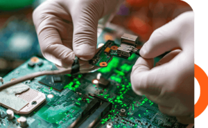
Kingda Lead-Free PCB Assembly Services
Kingda supports Lead-Free PCB Assembly for electronic products requiring lead-free soldering processes and controlled manufacturing.
The assembly workflow can include PCB fabrication, component sourcing, SMT placement, reflow soldering, through-hole assembly, inspection, electrical testing, and other production requirements according to the project specification.
Kingda can also support customers during the design and manufacturing preparation stages. DFM review and process evaluation can help identify potential assembly problems before production begins.
For projects requiring lead-free manufacturing, customers should provide the PCB design files, BOM, assembly drawings, component specifications, target market requirements, and any applicable compliance requirements. These documents allow the manufacturing process to be evaluated according to the actual product requirements.
Best Practices for Reliable Lead-Free PCB Assembly
For consistent production quality, manufacturers should consider the following practices:
- Select a solder alloy appropriate for the product and assembly process.
- Verify PCB and component temperature compatibility.
- Maintain strict separation between leaded and lead-free materials when both processes are used.
- Develop and validate the reflow profile.
- Control solder-paste storage and handling.
- Optimize stencil and pad design.
- Use SPI and AOI where appropriate for process monitoring.
- Apply X-ray inspection when hidden solder joints require inspection.
- Establish electrical and functional testing according to product requirements.
- Maintain material and process traceability throughout production.
Conclusion
Lead-Free PCB Assembly is now a standard manufacturing approach for many modern electronic products. Compared with traditional leaded soldering, lead-free assembly uses different solder alloys and generally requires higher processing temperatures and careful thermal management.
Reliable lead-free production depends on more than selecting a lead-free solder. PCB materials, components, solder paste, stencil design, reflow profiles, wave-soldering parameters, inspection, testing, and material control must all work together.
For manufacturers and product developers, the most effective approach is to evaluate lead-free requirements early in the design and manufacturing process. With appropriate material selection, process control, inspection, and engineering support, lead-free PCB Assembly can provide consistent manufacturing quality while meeting applicable environmental and customer requirements.