Massive MIMO PCB: Why 256TR Changes the Hard Part
On 3 September 2026 a Spanish operator and Ericsson completed a test of next generation mobile technology in the 6GHz band using a 256 transmit and receive antenna array, a clear step up from the 64 channel systems now common in deployed networks, and the trial also validated integrated sensing and communication. A massive MIMO PCB in that architecture has to keep several hundred radio channels electrically similar. Ericsson has listed that sensing capability among the defining features of the 6G stage, which means the network is expected to locate and identify objects as well as carry data.
For a massive MIMO PCB the significance of the trial is not the higher frequency by itself. It is that several hundred radio channels now have to behave almost identically on one board, and the phase errors that a small array could tolerate accumulate into a distorted beam. The manufacturing question changes from whether a radio path can reach fifty ohms to whether hundreds of them can hold the same impedance and propagation delay across a large panel.
What Actually Scales With Channel Count
Beamforming works by combining signals from many antenna elements with a defined amplitude and phase relationship. If the electrical length of one channel differs from another by a fraction of a wavelength, the combined pattern tilts or spreads. With sixty four channels the error budget is forgiving enough that conventional tolerance control is adequate. With two hundred and fifty six it is not.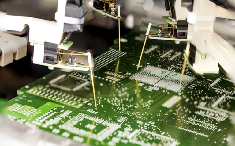
The error sources are unglamorous and all of them live on the board. Trace length differences change phase directly. Impedance variation changes the reflection behaviour of each channel. Dielectric thickness variation changes propagation velocity, so two channels routed the same length can still arrive at different times if the laminate beneath them differs. Copper surface condition adds another variable, because conductor loss depends on roughness.
Consistency Becomes a Fabrication Requirement
Manufacturers of radio boards have spent years optimising loss, because loss sets the link budget. Arrays of this size add a second requirement that is measured differently: dispersion, or how much the channels differ from one another. A board with excellent average loss but wide channel-to-channel variation will underperform a slightly lossier board with tight variation once beamforming is applied.
Delivering that means controlling the same parameters as before but to tighter limits: dielectric constant and thickness stability across the panel, etch precision so line widths match, registration between layers so via transitions behave consistently, and copper thickness uniformity over large areas. It also means measuring the result, which is why coupon structures placed at several positions on a production panel are more informative than a single test coupon at the edge. This is the sense in which high frequency manufacturing capability should be evaluated on distribution rather than on a best case number.
Why 6GHz Still Demands Careful Material Choice
The 6GHz band sits in a middle range where coverage and capacity can be balanced, and it avoids the propagation penalties of millimetre wave frequencies. It is not, however, low frequency. Dielectric and conductor losses consume a measurable share of the link budget, and the antenna feed network is long enough that loss accumulates before the signal reaches the radiating element.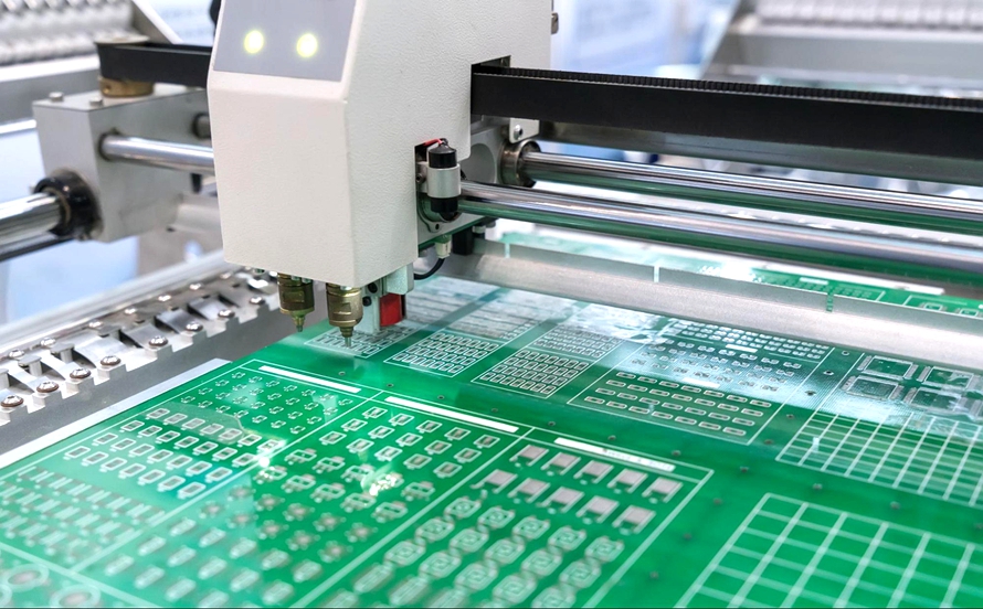
Designs therefore mix material classes. FR-4 remains adequate for baseband, control and low speed sections, while low dielectric constant and low loss factor laminates are used where the radio frequency path runs. That decision is not only about attenuation. A material with a stable dielectric constant makes the impedance calculation reliable in the first place, and it reduces the sensitivity of the design to small thickness variations introduced during lamination.
Copper Roughness and Large Panel Uniformity
At these frequencies the current concentrates near the surface of the conductor, so a rougher copper foil increases loss for the same trace geometry. Low profile foils reduce that effect and are standard in radio designs, but they also change how well the copper adheres to the laminate, which affects processing parameters.
Uniformity across the panel then becomes the practical problem. Plating thickness, etching rates and lamination pressure all vary slightly with position, and on a large antenna board those variations map directly onto channel characteristics. Factories building this class of work manage it by characterising the process across the panel, adjusting the layout of the antenna feed network to avoid the most variable regions where possible, and verifying coupons from several locations rather than assuming the panel is homogeneous.
Sensing Adds Isolation Requirements
Integrated sensing changes the electrical problem in a way that is easy to underestimate. A transmitted signal is strong, while the echo returned from a vehicle or a person is very weak, and both occupy the same hardware. The receive path has to detect that echo in the presence of leakage from the transmit path, which places heavy demands on channel isolation and on the linearity of the front end.
Board design contributes through partitioning. Transmit and receive sections need physical separation, ground structures have to provide return paths that do not couple between them, and any crosstalk path that was tolerable for communication alone becomes a limit on sensing range. In manufacturing terms, the same consistency requirement applies, because isolation depends on geometry and on the continuity of reference planes rather than on component selection.
Layering and Stack Up for Large Arrays
A 256 channel array needs a feed network, control and calibration paths for every channel, and power distribution, all on a board whose outline is set by the antenna spacing. Layer count rises because the radio frequency feed, the calibration network and the digital control interface cannot share the same layers without interfering.
Stack up design therefore allocates layers by function and keeps a continuous reference under every radio frequency path. Where a transition is unavoidable, it should be matched across all channels so the error remains common rather than differential. Designers who plan this at the beginning avoid the situation where a handful of channels need compensation in software because their routing could not be made to match the rest.
Calibration, Test and the Cost of Rework
Even a well made array needs calibration, and calibration tolerates a certain amount of variation. What it cannot repair is inconsistency that changes with temperature or time, because the phase correction applied at one condition becomes wrong at another. That is why material stability matters as much as initial accuracy.
Testing has to cover this dimension as well. Measuring one channel and assuming the rest are similar is not sufficient at this scale, and the practical approach is to characterise a sample of channels on each board, compare the distribution against production limits, and use that data to detect process drift. Investment in assembly and functional test pays for itself here, because a board that fails after integration costs far more than one caught at the factory.
Material Management Is Part of the Capability
When a design depends on dielectric consistency, the supplier’s material handling becomes part of the product specification. Batches from different production campaigns can differ slightly, and mixing them on one high speed panel introduces variation that no amount of process control can remove. Recording lot information and keeping campaigns separate on critical orders is good practice rather than an extra service.
That is also why the value of a radio frequency board supplier is increasingly described in terms of material management, stack up control and impedance compensation rather than the price of the laminate. Choosing a more expensive material without controlling its application produces less consistent results than applying a well understood material with disciplined process control, and it is the combination that a quality system is supposed to guarantee.
Panel Size and Handling Effects
An antenna board for a 256 channel array is physically large, and large panels behave differently from small ones during processing. Lamination pressure is distributed less evenly, material movement during thermal cycles is greater in absolute terms, and handling equipment designed for smaller formats can introduce scratches or edge damage on a panel that costs a great deal to make.
Suppliers with experience on this class of product usually invest in handling and in process characterisation across the panel long before they add capacity. For a customer, the useful question is not how big a panel the factory can process but how uniform the electrical result is from one edge of that panel to the other.
How Designers Reduce Sensitivity
Design has a role in making consistency achievable. Keeping radio frequency traces the same width and length where the layout permits, avoiding unnecessary layer transitions, and reserving a separate layer for the calibration network all reduce the number of variables that manufacturing has to control at once.
It also helps to keep impedance specifications realistic. Asking for a tolerance narrower than the process can hold does not improve the array; it creates rework and adds cost without changing the distribution of results. Matching the specification to demonstrated capability, and then verifying it with measurements, is the approach that produces boards which can be built in volume.
What the Next Generation of Base Stations Needs
The direction of travel is clear from the trial itself: more channels, more bands used together, and sensing functions layered on top of communication. Each of those trends increases the number of radio paths that must agree with each other, and none of them reduces the sensitivity of the design to manufacturing variation.
For manufacturers the preparation is concrete. Qualify low loss materials with stable dielectric properties, tighten etch and registration capability, build the measurement infrastructure to prove consistency across a panel, and treat material lot control as part of the process rather than as a warehouse concern. Equipment makers evaluating a partner for the next generation of radio platforms should ask for the distribution, not the average, and should expect the answer to come from a documented process rather than from a specification sheet.