Multilayer PCB Via Plugging Process and Quality Control
During multilayer PCB manufacturing, via plugging is an important process for maintaining PCB electrical performance, structural integrity, and long-term reliability. Vias provide critical electrical connections between different circuit layers, while proper filling helps protect the via structure, prevent contamination, and create a more stable surface for subsequent manufacturing processes.
Poor via plugging can result in internal voids, resin separation, surface depressions, cracks, and other defects. These problems may affect subsequent plating, surface finishing, component assembly, and the overall reliability of the finished PCB.
For this reason, an effective multilayer PCB via plugging quality-control system should cover material preparation, equipment setup, hole-wall treatment, filling, curing, planarization, inspection, and defect prevention.
For complex multilayer designs, these processes should also be evaluated together with the overall PCB stack-up, drilling, lamination, plating, and routing requirements. GOPCBA PCB Manufacturing
Overview of the Multilayer PCB Via Plugging Process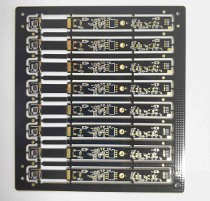
Via plugging is a PCB manufacturing process in which the internal space of a via is filled with a suitable material and, when required, the surface is subsequently planarized.
Common approaches include resin filling and copper electroplating. The appropriate method depends on the PCB structure, via dimensions, electrical requirements, thermal requirements, component packaging, and subsequent assembly processes.
Regardless of the selected process, high-quality via filling should generally achieve:
- Complete and uniform filling
- Minimal internal voids
- Strong adhesion to the hole wall
- Controlled surface height
- Good dimensional stability
- Compatibility with subsequent PCB processes
- Reliable electrical and mechanical performance
Proper filling is particularly important in high-density PCB designs. GOPCBA’s manufacturing capabilities include plugged vias, blind and buried vias, copper-filled microvias, and via-in-pad structures. Advanced PCB Manufacturing Capabilities
Key Quality-Control Steps for PCB Via Filling
Material and Equipment Preparation
Preparation is the foundation of a reliable PCB via filling process.
The filling material should be selected according to the via diameter, aspect ratio, PCB material, curing conditions, and subsequent manufacturing requirements. Resin materials should provide suitable viscosity, adhesion, thermal stability, and curing characteristics.
Before production, filling materials should be inspected for contamination, abnormal viscosity, deterioration, or other conditions that could affect filling performance.
Equipment should also be inspected and calibrated before processing. Depending on the manufacturing method, this may include:
- Vacuum plugging equipment
- Resin filling systems
- Grinding and planarization equipment
- Curing ovens
- Electroplating systems
- Cleaning equipment
Equipment cleanliness is equally important. Residual resin, dust, copper particles, or other contaminants can become trapped inside vias or remain on the PCB surface, creating defects in later processes.
Hole-Wall Pretreatment
Hole-wall preparation directly affects the adhesion and reliability of the filling material.
Before filling, the via should be thoroughly cleaned to remove:
- Drilling debris
- Dust
- Oil
- Oxides
- Moisture
- Other surface contamination
Depending on the PCB construction and process requirements, chemical cleaning, plasma treatment, desmear, or other suitable surface treatments may be used.
Proper surface conditioning improves the interaction between the hole wall and filling material. However, treatment parameters must be carefully controlled to prevent excessive copper removal, dimensional changes, or damage to the laminate structure.
After pretreatment, the hole-wall condition should be inspected before the PCB enters the filling process.
Filling and Curing Process Control
Filling is the core stage of the via filling process. The objective is to achieve complete filling without significant voids, bubbles, or unfilled areas.
For resin filling, vacuum-assisted filling can help remove trapped air and improve resin penetration into the via. Important parameters include resin viscosity, vacuum level, filling pressure, filling speed, and material temperature.
For copper-filled vias, electroplating parameters must be carefully controlled to promote uniform copper deposition throughout the via structure.
After filling, curing stabilizes the material and strengthens its connection with the surrounding PCB structure.
Curing temperature and time should be controlled according to the material specification. Insufficient curing may result in weak adhesion or material deformation, while excessive or poorly controlled curing may increase shrinkage and create cracks.
After curing, the filled vias should undergo an initial inspection for obvious surface defects such as protrusions, depressions, cracks, or incomplete filling.
Surface Grinding and Planarization
After curing, excess filling material may remain above the PCB surface. Grinding or other planarization processes are used to remove the excess material and create a more uniform surface.
The goal is to achieve a flat surface suitable for subsequent PCB fabrication and assembly.
Grinding parameters must be carefully controlled. Excessive grinding can damage surrounding copper or laminate, while insufficient grinding can leave material protruding from the PCB surface.
After planarization, the PCB should be thoroughly cleaned to remove:
- Grinding dust
- Resin particles
- Copper debris
- Other contaminants
Surface flatness becomes particularly important when filled vias are associated with fine-pitch components or via-in-pad structures. GOPCBA supports via-in-pad manufacturing as part of its advanced PCB fabrication capabilities. GOPCBA PCB Manufacturing Services
Common Via Plugging Defects and Prevention
Voids and Air Bubbles
Voids and air bubbles are common problems in via filling. They can result from insufficient vacuum, inappropriate material viscosity, trapped moisture, contamination, or unstable filling parameters.
Preventive measures include:
- Selecting suitable filling materials
- Controlling material viscosity
- Optimizing vacuum and pressure parameters
- Properly drying PCB materials
- Thoroughly cleaning the via
- Maintaining stable filling conditions
For advanced multilayer structures, internal defects may require X-ray or cross-sectional analysis because they cannot always be identified through visual inspection.
Surface Depressions
Surface depressions may result from resin shrinkage, insufficient filling volume, or excessive grinding.
Control measures include optimizing the filling volume, controlling curing conditions, and establishing appropriate grinding parameters.
Where permitted by the product specification, minor surface defects may be corrected through controlled secondary filling and planarization.
Resin Separation and Plating Delamination
Resin separation or copper plating delamination can occur when the hole wall has not been properly cleaned or conditioned, or when the filling material is incompatible with the PCB structure.
The main preventive measures include:
- Improving hole-wall cleaning
- Optimizing surface conditioning
- Selecting compatible filling materials
- Controlling curing conditions
- Stabilizing electroplating parameters
For copper-filled vias, plating uniformity and adhesion are especially important for long-term electrical and mechanical reliability.
Hole and Surface Contamination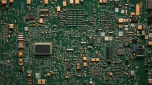
Contamination may come from equipment residue, production dust, improper handling, or insufficient cleaning.
Manufacturing equipment should be cleaned regularly, while production areas should be controlled to minimize airborne particles and other contaminants.
Operators should also follow standardized handling procedures to prevent contamination from entering vias or contacting critical PCB surfaces.
Establishing a Complete Via Filling Quality-Control System
Effective multilayer PCB manufacturing requires quality control throughout the entire via plugging process rather than relying only on final inspection.
A standardized process should define:
- Material specifications
- Equipment parameters
- Hole-wall preparation requirements
- Filling conditions
- Curing parameters
- Grinding and planarization requirements
- Inspection criteria
- Defect classification
- Rework procedures
- Final acceptance standards
Process inspection should be performed at critical manufacturing stages so that defects can be identified and corrected before they move into subsequent processes.
Operator training is also important. Production personnel should understand process parameters, equipment operation, common defect patterns, inspection requirements, and corrective actions.
Regular equipment maintenance and calibration are equally necessary to maintain stable vacuum, pressure, temperature, plating, and grinding performance.
Inspection and Testing for Via Plugging Quality
Inspection methods should be selected according to the PCB structure and reliability requirements.
Visual inspection can identify obvious surface defects, contamination, excessive filling material, and poor planarization.
Dimensional inspection can verify PCB thickness, via dimensions, surface flatness, and other mechanical characteristics.
For advanced multilayer boards, X-ray inspection can help identify hidden internal structures and potential defects. Cross-sectional analysis can provide more detailed information about via filling, copper plating, hole-wall condition, and layer alignment.
Electrical testing can then verify circuit continuity and isolation after fabrication.
GOPCBA’s published quality-management information states that its PCB manufacturing process includes high-quality raw materials, advanced manufacturing and testing equipment, professional technical support, and 100% electrical testing. GOPCBA Quality Management
Via Filling in HDI and High-Density PCB Manufacturing
As electronic products become smaller and more functional, via filling has become increasingly important in advanced PCB technologies.
HDI PCB manufacturing uses fine lines, microvias, blind vias, buried vias, and sequential buildup structures to increase circuit density while reducing board size. These structures require tighter control of drilling, plating, lamination, and via filling processes.
GOPCBA’s HDI capabilities include microvias, stacked microvias, copper-filled microvias, buried filled vias, and multilayer buildup structures. GOPCBA HDI PCB Design and Manufacturing Guide
For resin plugged vias, the filling process must be matched to the PCB stack-up and subsequent surface-finishing requirements. For copper-filled microvias, plating uniformity and reliability become additional process considerations.
Via filling is also closely related to fine-pitch BGA routing, high-density interconnects, and via-in-pad applications. Properly filled and planarized vias can help provide a stable surface for component placement and soldering.
Process Integration with PCB Design and Manufacturing
Via plugging should not be treated as an isolated manufacturing operation.
During engineering review, manufacturers should evaluate the relationship between via size, aspect ratio, pad dimensions, stack-up, copper thickness, dielectric thickness, plating requirements, and subsequent assembly.
Early DFM analysis can help identify manufacturing risks before production begins. GOPCBA provides engineering support covering PCB design review, DFM/DFA analysis, stack-up optimization, and manufacturing feasibility evaluation. GOPCBA PCB Manufacturing and DFM Support
This integrated approach is particularly valuable for HDI, high-layer-count, fine-pitch, and other advanced PCB designs where a small process deviation can affect multiple manufacturing stages.
Conclusion
Via plugging is an important process in multilayer PCB manufacturing, especially for high-density and advanced PCB structures. Reliable results depend on coordinated control of materials, hole-wall preparation, filling, curing, planarization, inspection, and equipment performance.
A robust quality-control system should monitor the complete process rather than relying solely on final inspection. By controlling critical parameters, identifying defects at each stage, maintaining equipment stability, and applying appropriate inspection methods, manufacturers can improve PCB consistency, electrical reliability, and long-term performance.
As PCB designs continue to evolve toward higher density, smaller features, and more complex interconnections, reliable PCB via filling will remain an important part of advanced PCB fabrication.