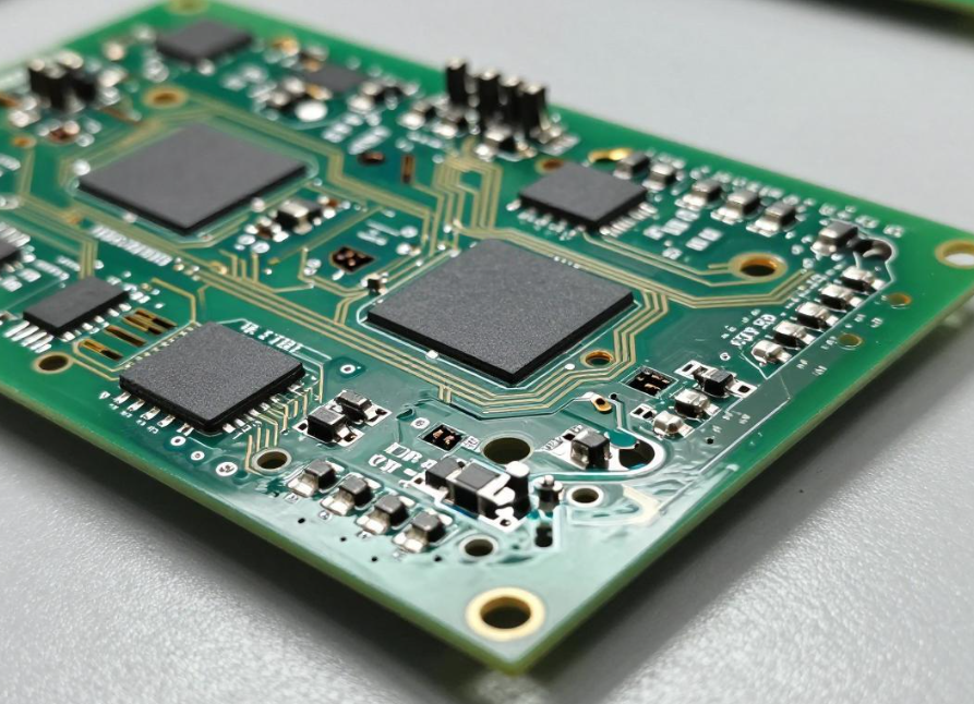
OSP, or Organic Solderability Preservative, is widely used in consumer electronics, industrial control equipment, communication boards, and other applications because it provides a relatively flat soldering surface, supports fine-pitch BGA and QFN assembly, and can offer a cost-effective surface-finish solution.
However, a common production problem is that prototype boards may pass soldering and storage verification while oxidation or solderability problems emerge after the project enters mass production.
This does not necessarily mean that storage conditions are the only cause. The long-term stability of an OSP PCB depends on multiple factors, including copper-surface preparation, OSP chemical processing, coating uniformity, surface contamination, packaging, transportation, storage, and assembly thermal exposure.
Because the OSP coating is extremely thin, relatively small variations in surface preparation or coating conditions can affect its protective performance. Some defects may not be obvious during outgoing inspection but can become more significant during storage, transportation, repeated reflow, or rework.
For this reason, OSP surface finish reliability should be evaluated as a complete manufacturing and application system rather than through coating thickness alone.
1. OSP Film Structure and Applicable Industry Requirements
OSP is formed when organic compounds react with the exposed copper surface to create a protective organic layer. Depending on the chemistry, the organic molecules can form a coordinated or adsorbed protective structure on the copper surface.
The purpose of the coating is to reduce direct exposure of copper to oxygen, moisture, and contaminants before soldering. During the soldering process, the coating is displaced or decomposed under the combined influence of heat and flux, allowing solder to contact the underlying copper.
For OSP PCB production, average coating thickness alone does not fully describe surface-finish quality.
Engineers should also consider:
- Coating uniformity
- Surface cleanliness
- Copper pretreatment
- Coating continuity
- Chemical bath stability
- Rinsing quality
- Drying conditions
- Solderability after environmental exposure
- Packaging and storage conditions
OSP thickness ranges depend on the chemistry and manufacturer’s process window. Therefore, values such as 0.2–0.5 μm should be treated as process-specific references rather than universal industry requirements.
A coating that is too thin may provide insufficient protection under certain storage conditions, while an excessively thick or improperly formed coating may affect solderability.
The appropriate acceptance range should therefore be established according to the selected OSP chemistry, supplier specification, applicable standard, and customer solderability requirements.
For mass production, controlling coating variation within the panel and between production batches can be more meaningful than evaluating only the nominal average value.
2. Typical Engineering Symptoms of OSP Oxidation Failure
2.1 Localized Yellowing or Darkening of Pads
Early-stage PCB oxidation may appear as subtle yellowing, darkening, or discoloration of exposed copper pads.
Because the visual change can be relatively minor, it may not be identified during routine incoming inspection.
At the microscopic level, insufficient coating continuity, surface contamination, or localized coating degradation can expose copper to moisture and oxygen.
The resulting surface condition may still allow soldering during an initial reflow cycle but become more difficult to solder after extended storage or additional thermal exposure.
Dense BGA arrays, isolated fine-pitch pads, and areas with unfavorable process access may require additional attention during failure analysis.
2.2 Severe Oxidation and Poor Solder Wetting
A more serious failure occurs when exposed copper becomes significantly oxidized.
Severe PCB oxidation can reduce solder wetting and spreading, increasing the risk of non-wetting, dewetting, insufficient solder joints, or open connections.
If a large portion of a production batch exhibits the same condition, the root cause should be investigated across the entire process chain rather than attributed immediately to customer storage.
Potential causes include coating defects, contamination, packaging damage, moisture exposure, unsuitable storage conditions, or excessive thermal history.
2.3 Uneven Oxidation Within the Same Batch
Another important symptom is inconsistent oxidation.
Some boards may remain visually acceptable while others from the same production batch show discoloration. On an individual board, the edge may appear different from the center, while dense pad regions may behave differently from larger exposed copper areas.
This pattern can indicate variation in surface preparation, OSP solution exchange, panel positioning, coating uniformity, handling, or packaging exposure.
The distribution pattern is therefore valuable information during OSP failure analysis.
2.4 Solderability Decline After Repeated Thermal Exposure
OSP is a protective surface treatment designed to preserve the solderability of copper before assembly. Its condition changes during soldering.
Repeated reflow and rework can therefore reduce the remaining protection and alter the copper surface.
It is not appropriate to specify one universal maximum number of reflow cycles for every OSP material. The actual limit depends on the OSP chemistry, coating condition, thermal profile, peak temperature, time above liquidus, flux chemistry, atmosphere, and assembly sequence.
For double-sided SMT, minimizing unnecessary thermal exposure and avoiding long storage intervals between assembly operations can help maintain more consistent solderability.
When repeated reflow or rework is expected, the actual production thermal profile should be included in solderability validation.
2.5 Sulfur-Related Discoloration
Sulfur-containing environments can also contribute to copper surface discoloration.
If the OSP protection is compromised and exposed copper comes into contact with sulfur-containing contaminants, copper sulfide or related corrosion products may form, producing gray, brown, or black surface discoloration.
This mechanism should be distinguished from ordinary oxidation because the environmental chemistry and failure mechanism are different.
Communication equipment, industrial enclosures, and other products exposed to specific atmospheric contaminants may require additional environmental assessment.
3. Root Causes of Unstable OSP Oxidation Resistance
3.1 Inconsistent Copper Surface Preparation
A stable OSP surface finish begins with a clean and chemically consistent copper surface.
If degreasing, micro-etching, activation, or rinsing varies across the panel, the copper surface may have different levels of contamination, roughness, oxide condition, or surface activity.
The OSP molecules may therefore react differently in different regions.
During prototype production, low production volume and fresh process chemistry may make process variation less obvious. During continuous mass production, bath loading, chemical consumption, contamination, and process drift can become more significant.
For this reason, copper pretreatment is a critical control point for OSP PCB reliability.
3.2 Chemical and Fluid-Dynamic Variation During Coating
OSP coating is a wet chemical process, so solution exchange and surface accessibility can affect local coating conditions.
Large exposed copper areas, isolated small pads, dense BGA arrays, and panel-edge regions may experience different solution-flow conditions.
This does not mean that the center of every panel will necessarily have a thinner coating than its edges. Actual results depend on the equipment, process configuration, panel orientation, agitation, chemical concentration, temperature, and production conditions.
Nevertheless, unusual pad distributions and highly uneven copper exposure should be reviewed during DFM.
3.3 Ionic Contamination and Surface Residues
After OSP treatment, inadequate rinsing or poor process control may leave residues from the chemical process on the PCB surface.
Potential contaminants can include ionic residues, copper-containing species, or decomposition products.
Under humid conditions, ionic contamination can contribute to electrochemical reactions and corrosion, potentially reducing the long-term effectiveness of the protective layer.
Because this type of failure may develop gradually during storage, visual inspection alone may not identify the underlying cause.
Ion cleanliness testing and appropriate environmental reliability testing can therefore be useful when contamination is suspected.
3.4 Thermal Damage to the OSP Coating
The OSP coating has a limited thermal process window.
Excessive drying temperature, excessive thermal exposure during manufacturing, or unsuitable customer-side baking can alter the organic protective layer.
This can reduce its ability to protect the copper during subsequent storage.
Therefore, drying and baking conditions should follow the selected OSP chemistry and supplier’s process recommendations.
OSP boards should not automatically be subjected to the same baking conditions used for conventional bare copper or other surface finishes.
3.5 Mechanical Damage During Packaging and Handling
OSP films are extremely thin and can be damaged by repeated friction.
If boards are stacked directly against each other without suitable separation, exposed pads can rub against neighboring boards during packaging and transportation.
Once the coating is locally damaged, the underlying copper becomes more vulnerable to environmental exposure.
Packaging should therefore be treated as part of PCB oxidation prevention rather than as a purely logistical operation.
4. Engineering Risk Checklist Before Mass Production
Before approving an OSP PCB for mass production, engineers should review the following areas:
- Define the OSP chemistry and applicable surface-finish requirements.
- Confirm the coating-thickness range specified by the OSP supplier.
- Review coating uniformity and production control methods.
- Define solderability acceptance criteria after relevant environmental exposure.
- Verify copper-surface preparation and cleaning requirements.
- Evaluate BGA, QFN, and other dense fine-pitch pad regions.
- Review panelization and potential edge-related process variation.
- Confirm packaging and moisture-protection requirements.
- Establish storage and open-package exposure limits.
- Evaluate the planned reflow and rework thermal history.
Prototype approval should not automatically be considered proof of mass-production stability.
A prototype may pass because of favorable material lots, fresh chemical baths, limited storage time, or a different production configuration. A proper pilot-production evaluation provides a better indication of whether the process remains stable under volume manufacturing conditions.
5. OSP Quality Control Should Go Beyond Visual Inspection
Visual inspection is useful for identifying obvious discoloration, scratches, contamination, and surface defects, but it cannot fully characterize the protective performance of an OSP surface finish.
Depending on the application, quality control can combine:
- Visual inspection
- Coating-thickness verification where applicable
- Surface cleanliness testing
- Solderability testing
- Environmental aging
- Steam aging where specified
- Thermal cycling
- Ionic contamination testing
- Cross-sectional or microscopic analysis during failure investigation
The specific tests and acceptance limits should be established according to the customer specification, applicable standards, OSP supplier requirements, and product reliability targets.
For high-volume products, periodic verification of representative production batches can help identify process drift before it becomes a customer-level failure.
6. Connecting OSP Process Control With Packaging and Storage
The PCB oxidation risk does not end when the OSP process is completed.
A complete control chain should include:
Copper preparation → OSP coating → rinsing → drying → inspection → packaging → transportation → storage → SMT assembly
A defect introduced during surface preparation may be amplified by long-term storage.
A good OSP coating can also be damaged by unsuitable packaging.
Similarly, properly packaged boards can still experience solderability problems if they are exposed to excessive humidity or remain unpacked for too long.
This means that responsibility for OSP PCB reliability should be shared across engineering, PCB manufacturing, quality control, logistics, and SMT assembly teams.
7. Kingda’s OSP PCB Engineering and Manufacturing Support
Kingda can support OSP projects through integrated engineering and manufacturing control.
During the pre-production stage, the PCB layout, panelization, exposed-copper distribution, BGA/QFN regions, tooling structures, and manufacturing requirements can be reviewed to identify potential risks.
During production, the OSP process, copper pretreatment, coating consistency, cleaning, drying, inspection, and packaging requirements should be controlled according to the approved specification.
For demanding applications, pilot production and solderability validation can be used to verify whether the selected OSP surface finish remains stable under actual storage and SMT conditions.
By combining DFM review, process control, packaging protection, and application-specific validation, Kingda helps customers reduce the risk of PCB oxidation, solderability degradation, and batch-level failures during mass production.