In modern electronics manufacturing, PCBA testing is a critical part of quality control used to verify whether an assembled printed circuit board meets its electrical, functional, and reliability requirements before shipment.
A PCB assembly may appear visually perfect after SMT and THT assembly, yet hidden problems such as soldering defects, incorrect component values, open circuits, short circuits, poor solder joints, and signal integrity issues can still affect product performance. Without an effective PCB assembly testing strategy, these defects may eventually result in field failures, warranty claims, product recalls, and increased manufacturing costs.
Effective PCBA testing is therefore not simply a final inspection step. It is a systematic quality-control process that begins with incoming materials and continues through PCB assembly, soldering, inspection, electrical testing, functional verification, and final quality inspection.
For complex and high-density electronic products, manufacturers need a combination of inspection and testing technologies rather than relying on a single test method. SPI, AOI, X-ray inspection, Flying Probe Testing, ICT, Functional Circuit Testing, and reliability testing each identify different categories of defects.
As an experienced PCB manufacturer and PCB assembly service provider, Kingda provides PCB prototype manufacturing, rapid PCB prototyping, PCB fabrication, component sourcing, SMT assembly, THT assembly, inspection, testing, and production support. This integrated capability helps customers move from initial design verification to small-batch production and volume manufacturing while maintaining consistent quality control.
This guide explains what PCBA testing is, why it matters, the difference between PCB inspection and PCB testing, the major testing methods, common PCBA defects, how to select an appropriate testing strategy, and how Kingda integrates testing into the PCB assembly process.
What Is PCBA Testing?
PCBA testing is the process of inspecting, measuring, and validating a printed circuit board assembly after electronic components have been mounted and soldered onto the PCB.
Unlike a visual inspection that primarily identifies physical or visible defects, PCB testing verifies whether electrical connections, component characteristics, circuit operation, and system functions meet the original design requirements.
A complete PCBA testing process may include:
- Visual inspection
- Solder Paste Inspection (SPI)
- Automated Optical Inspection (AOI)
- Automated X-Ray Inspection (AXI)
- Flying Probe Testing (FPT)
- In-Circuit Testing (ICT)
- Functional Circuit Testing (FCT)
- Insulation and withstand voltage testing
- Environmental and reliability testing
The appropriate combination depends on the PCB design, component density, production volume, application environment, product risk, and customer requirements.
How PCBA Testing Fits into the Manufacturing Process
A typical electronics manufacturing workflow includes:
PCB Design → DFM Review → PCB Manufacturing → Incoming Quality Control → SMT/THT Assembly → SPI/AOI/X-Ray Inspection → Electrical Testing → Functional Testing → Final Inspection → Packaging & Shipment
PCB fabrication produces the bare circuit board, while PCB assembly mounts electronic components onto the board. After soldering, different inspection and testing methods are used to verify assembly quality and electrical performance.
Testing data can also be fed back into the manufacturing process. For example, recurring solder defects may indicate an incorrect reflow profile, stencil design problem, solder paste issue, or component-placement deviation.
Main Objectives of PCBA Testing
The primary objectives of PCB assembly testing include:
- Detecting manufacturing defects before shipment
- Verifying electrical connectivity
- Confirming component values and polarity
- Identifying soldering defects
- Verifying circuit functionality
- Improving manufacturing yield
- Supporting regulatory and customer requirements
- Reducing warranty and field-failure costs
- Improving production-process stability
- Providing traceability for critical products
Kingda integrates inspection and testing into its PCB assembly manufacturing workflow, allowing potential problems to be identified as early as possible rather than waiting until final assembly or field operation.
Why Is PCB Assembly Testing Important?
PCB assembly testing is essential because not every manufacturing defect can be detected through visual inspection alone. A board can look acceptable while containing an internal solder void, incorrect resistance value, intermittent connection, or hidden BGA solder defect.
Testing provides objective evidence that an assembled PCB performs according to its design requirements.
1. Preventing Costly Product Failures
Detecting a defective PCBA during manufacturing is generally much less costly than discovering the same failure after the product has been shipped.
Effective testing can help reduce:
- Field failures
- Warranty claims
- Customer complaints
- Product returns
- Rework costs
- Scrap
- Product recalls
- Technical support costs
Early detection also allows engineers to correct the root cause before the same defect is repeated across a larger production batch.
2. Improving Manufacturing Yield
Test results provide valuable production data.
For example, repeated defects in the same location may indicate:
- Solder paste-printing problems
- Incorrect stencil aperture design
- Component-placement deviation
- Reflow-profile instability
- PCB warpage
- Component quality issues
- Incorrect assembly parameters
By analyzing this information, manufacturers can continuously improve the production process and increase PCBA manufacturing yield.
3. Supporting Industry Standards
Depending on the application, electronic assemblies may need to comply with standards and customer specifications such as IPC-A-610, IPC/WHMA-A-620, ISO 9001, ISO 13485, automotive quality requirements, or other industry-specific requirements.
The applicable standard should always be confirmed according to the product, market, customer specification, and intended application.
4. Increasing Product Reliability
A comprehensive PCBA testing strategy provides multiple layers of protection.
For example:
- SPI verifies solder paste deposition
- AOI verifies component placement and visible solder defects
- X-ray verifies hidden solder joints
- ICT checks electrical characteristics
- FCT verifies overall product operation
- Reliability testing evaluates performance under environmental stress
Together, these methods provide much broader defect coverage than any single inspection technology.
PCB Inspection vs. PCB Testing
PCB inspection and PCB testing are related but serve different purposes.
| PCB Inspection | PCB Testing |
|---|---|
| Primarily detects physical and assembly defects | Verifies electrical and functional performance |
| Uses cameras, optical systems, or X-ray systems | Uses probes, fixtures, instruments, and test software |
| Checks component placement and solder joints | Checks continuity, component values, signals, and functions |
| Can be performed throughout assembly | Usually performed at defined electrical or functional stages |
| Focuses on physical quality | Focuses on electrical and functional behavior |
PCB Inspection
Common PCB inspection methods include:
- Manual Visual Inspection
- SPI
- AOI
- X-ray Inspection
These technologies can identify problems such as missing components, incorrect polarity, solder bridges, insufficient solder, misalignment, solder voids, and hidden solder-joint defects.
PCB Testing
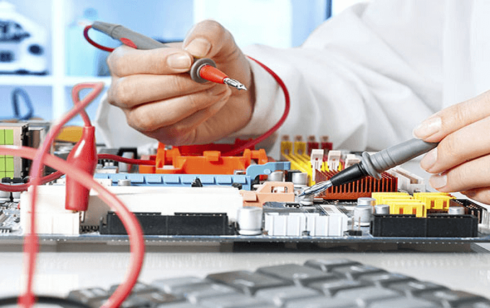
PCB testing applies electrical signals or test conditions to the assembled circuit and evaluates its response.
Typical methods include:
- Flying Probe Testing
- In-Circuit Testing
- Functional Circuit Testing
- Continuity testing
- Insulation resistance testing
- Dielectric withstand testing
- Reliability testing
Inspection and testing should therefore be viewed as complementary processes rather than competing alternatives.
Types of PCBA Testing
No single PCBA test method can identify every possible manufacturing or functional problem.
Modern PCB assembly manufacturers therefore combine multiple inspection and testing methods according to production volume, PCB complexity, component technology, product risk, and customer requirements.
1. Solder Paste Inspection (SPI)
Solder Paste Inspection (SPI) is performed after solder paste printing and before component placement.
SPI equipment measures solder paste characteristics such as:
- Volume
- Height
- Area
- Position
- Shape
- Offset
The objective is to identify printing problems before components are placed.
Typical defects include:
- Insufficient solder paste
- Excessive solder paste
- Misaligned paste deposits
- Uneven deposits
- Bridging risks
- Blocked stencil apertures
Because solder paste printing directly affects solder-joint quality, SPI testing is an important early-stage control point in SMT manufacturing.
2. Automated Optical Inspection (AOI)
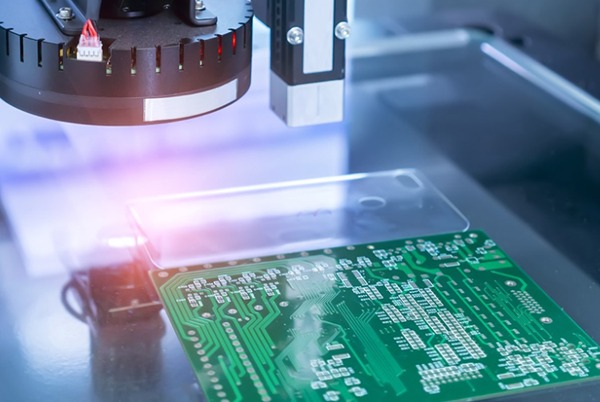
Automated Optical Inspection (AOI) uses cameras and image-processing technology to inspect assembled PCBs.
AOI can identify many visible defects, including:
- Missing components
- Incorrect components
- Component misalignment
- Incorrect polarity
- Tombstoning
- Lifted leads
- Solder bridges
- Insufficient visible solder
- Excessive solder
- Incorrect component orientation
AOI can be performed before or after reflow depending on the manufacturing process.
Pre-Reflow AOI
Pre-reflow AOI focuses primarily on component presence, position, orientation, and polarity.
Detecting defects before reflow can reduce the need for later rework.
Post-Reflow AOI
Post-reflow AOI is commonly used to inspect component placement and visible solder-joint characteristics after soldering.
However, AOI has an important limitation: it cannot directly see solder joints hidden beneath packages.
This is why dense packages such as BGA, QFN, LGA, and other bottom-terminated components may require X-ray inspection.
3. Automated X-Ray Inspection (AXI)
Automated X-Ray Inspection (AXI) uses X-ray imaging to inspect structures that cannot be viewed directly from the PCB surface.
It is particularly useful for:
- BGA solder joints
- QFN thermal pads
- LGA packages
- Hidden solder connections
- Voids
- Internal shorts
- Insufficient solder
- Component alignment
Why Is X-Ray Inspection Important?
As PCB designs become smaller and component density increases, more solder joints are hidden beneath component packages.
A board may pass AOI while still containing defects underneath a BGA.
X-ray inspection provides a non-destructive method for examining these hidden areas.
Advanced X-ray systems can provide detailed images of solder structures and help engineers evaluate voiding, bridging, insufficient solder, and other internal defects.
4. Flying Probe Testing (FPT)
Flying Probe Testing uses movable probes to contact designated test points on the PCB.
Unlike ICT, Flying Probe Testing generally does not require a dedicated bed-of-nails fixture.
It is particularly suitable for:
- PCB prototypes
- Engineering validation
- Small-batch PCB assembly
- Low-volume production
- Frequently changing designs
Typical tests include:
- Opens
- Shorts
- Continuity
- Resistance
- Capacitance
- Diode characteristics
- Selected component parameters
The main advantage is flexibility. The main limitation is that testing can take longer per board compared with a dedicated ICT fixture.
For PCB prototype manufacturing and low-volume production, Flying Probe Testing can therefore be an efficient solution when fixture investment needs to be minimized.
5. In-Circuit Testing (ICT)
In-Circuit Testing (ICT) uses a dedicated fixture to contact test points on the assembled PCB.
It can verify various electrical characteristics, including:
- Resistance
- Capacitance
- Diode polarity
- Component presence
- Opens
- Shorts
- Selected transistor and IC characteristics
ICT is particularly suitable for mature products with relatively stable designs and medium- to high-volume production.
Its major advantages include:
- Fast testing
- Repeatability
- High automation
- Broad electrical defect coverage
The main consideration is the initial cost of developing a dedicated test fixture.
6. Functional Circuit Testing (FCT)
Functional Circuit Testing (FCT) evaluates whether the complete PCBA performs according to its intended operating requirements.
Instead of testing individual components separately, FCT powers the board and evaluates its behavior under defined operating conditions.
Depending on the product, functional testing may verify:
- Power-up behavior
- Communication interfaces
- Sensor signals
- Display functions
- Motor control
- Relay operation
- Analog outputs
- Digital outputs
- Wireless communication
- Firmware-controlled functions
For example, an FCT procedure may verify whether a controller communicates correctly with another device, whether sensor data remains within the specified range, or whether an output signal has the expected frequency and amplitude.
FCT is therefore particularly important when a product’s final performance depends on multiple circuits working together.
7. Reliability Testing
For products that must operate reliably under demanding conditions, PCBA reliability testing can supplement standard electrical testing.
Typical reliability tests include:
- Thermal cycling
- High-temperature operation
- Low-temperature operation
- Humidity exposure
- Temperature-humidity testing
- Vibration testing
- Mechanical shock
- Burn-in
- Connector mating-cycle testing
- Bending or flex testing where applicable
The exact test conditions should be established according to the product’s intended environment and applicable standards.
Common Defects Detected During PCBA Testing
Different PCBA testing methods identify different defect types.
Solder Bridges
A solder bridge occurs when solder unintentionally connects adjacent conductive areas.
It can create an electrical short and cause circuit malfunction.
Common detection methods include:
- AOI
- X-ray inspection
- ICT
- FCT
Open Circuits
An open circuit occurs when an electrical connection that should exist is interrupted.
Possible causes include:
- Insufficient solder
- Cracked solder joints
- Damaged traces
- Poor component termination
- Incorrect component placement
Continuity testing, Flying Probe Testing, ICT, and FCT can help identify these failures.
Missing or Misaligned Components
Incorrect component placement can prevent the circuit from operating correctly.
AOI can detect:
- Missing components
- Misalignment
- Incorrect orientation
- Polarity errors
- Tombstoning
- Lifted components
Cold or Weak Solder Joints
Poor solder wetting or insufficient soldering can create mechanically weak or electrically unstable connections.
Depending on the component structure, detection may involve:
- AOI
- X-ray
- Electrical testing
- Functional testing
- Microscopic inspection
Incorrect Component Values
A resistor or capacitor with an incorrect value may cause the circuit to behave differently from the design.
Depending on the component and circuit configuration, ICT, Flying Probe Testing, LCR measurement, or functional testing can help identify incorrect values.
Hidden BGA Solder Defects
BGA solder joints cannot be directly inspected using conventional optical inspection.
Potential problems include:
- Voids
- Bridging
- Opens
- Insufficient solder
- Misalignment
X-ray inspection is therefore an important tool for assemblies containing BGA and other hidden solder connections.
Functional Failures
Some PCBAs may pass visual inspection and basic electrical tests but still fail during actual operation.
Possible causes include:
- Firmware problems
- Timing issues
- Signal integrity problems
- Incorrect circuit behavior
- Communication failures
- Sensor calibration issues
These problems are best evaluated through Functional Circuit Testing and application-specific validation.
How to Choose the Right PCBA Testing Method
The appropriate PCB assembly testing strategy depends on several factors.
1. Production Volume
Production volume strongly influences the choice of testing technology.
Low-volume and prototype production may benefit from Flying Probe Testing because it avoids the need for a dedicated ICT fixture.
High-volume production may justify ICT fixtures because the cost can be distributed across a larger number of units and test times can be reduced.
2. PCB Complexity
High-density PCBs with:
- BGA
- QFN
- Fine-pitch components
- Multilayer structures
- High component density
- Hidden solder joints
may require a combination of:
SPI + AOI + X-ray + ICT/Flying Probe + FCT
The greater the design complexity, the more important it becomes to use complementary inspection and testing technologies.
3. Product Reliability Requirements
Testing requirements vary significantly by application.
For example:
- Consumer electronics may prioritize production efficiency and cost
- Industrial electronics may require greater environmental durability
- Automotive electronics may require extensive electrical and environmental validation
- Medical electronics may require strict traceability and documented quality processes
- Aerospace and other high-reliability applications may require additional verification according to customer and regulatory requirements
4. Cost Considerations
Testing should balance product risk, production volume, test coverage, and investment.
A low-cost testing strategy may reduce manufacturing expense initially but could increase the risk of field failures.
A well-designed PCBA quality control system focuses on preventing defects as early as possible while selecting appropriate tests for the actual risk profile of the product.
Advantages of PCBA Testing
A comprehensive PCBA testing strategy provides benefits beyond simple defect detection.
Improved Product Quality
Testing verifies assembled boards against defined electrical and functional requirements before shipment, improving consistency between production batches.
Reduced Manufacturing Costs
Early detection prevents defective boards from moving through additional production stages and reduces unnecessary rework and scrap.
Improved Process Control
Test data helps engineers identify recurring issues in:
- Solder paste printing
- Component placement
- Reflow soldering
- Component sourcing
- PCB fabrication
- Assembly processes
Increased Customer Confidence
Consistent testing and documented inspection results provide customers with greater confidence in product quality and production consistency.
Better Traceability
For applications requiring strict quality management, test records can support batch tracking, process analysis, failure investigation, and after-sales service.
Reduced Field Failures
Identifying defects before shipment reduces the probability that defective PCBAs will reach the final product or end user.
Applications of PCB Assembly Testing
Different industries require different levels and combinations of PCB assembly testing.
1. Consumer Electronics
Consumer products such as:
- Smart home devices
- Wearables
- Gaming equipment
- Audio products
- IoT devices
often require AOI, electrical testing, and functional testing.
For high-volume production, automated testing can help maintain consistent throughput and quality.
2. Automotive Electronics
Automotive PCBAs are used in:
- ECUs
- Battery management systems
- ADAS
- Infotainment systems
- Sensors
- Lighting controllers
- Power electronics
These applications may require a combination of AOI, X-ray, ICT, FCT, electrical safety testing, and reliability testing according to the product’s risk and applicable automotive requirements.
3. Medical Electronics
Medical devices require a strong focus on:
- Reliability
- Traceability
- Electrical safety
- Process control
- Documentation
Applications include:
- Patient monitoring equipment
- Diagnostic instruments
- Imaging equipment
- Laboratory equipment
- Surgical electronics
Kingda can support customers requiring controlled PCB assembly and testing for medical electronics, with manufacturing processes aligned with applicable customer specifications and quality-system requirements.
4. Industrial Automation
Industrial PCBAs are commonly used in:
- PLCs
- Servo controllers
- Robotics
- Industrial sensors
- Motor drives
- Power-control systems
- Communication equipment
Because industrial equipment may operate continuously and under vibration, temperature variation, dust, or electrical noise, PCB assembly testing should be selected according to the actual operating environment.
Kingda PCBA Testing and PCB Assembly Capabilities
As an experienced PCB manufacturer and PCB assembly service provider, Kingda provides an integrated manufacturing solution covering the complete product development and production cycle.
Our capabilities can support customers from initial PCB design verification through prototype manufacturing, assembly, inspection, testing, and volume production.
PCB Manufacturing
Kingda provides PCB prototype manufacturing and PCB fabrication for different application requirements, supporting customers during design verification and product development.
PCB Assembly
Our PCB assembly services can integrate:
- SMT assembly
- THT assembly
- Mixed technology assembly
- Component sourcing
- Prototype PCBA
- Small-batch PCBA
- Production PCBA
Quality Inspection
Depending on project requirements, the quality-control workflow can incorporate:
- Incoming inspection
- SPI
- AOI
- X-ray inspection
- Visual inspection
- Electrical testing
- Functional testing
Engineering Support
Kingda supports customers throughout the transition from prototype to production by helping evaluate:
- PCB design
- Component selection
- BOM information
- Assembly requirements
- Test requirements
- Manufacturing considerations
This integrated approach helps reduce communication gaps between PCB fabrication, component procurement, assembly, and testing.
Prototype to Volume Production
For customers developing new electronic products, Kingda can support the complete manufacturing path:
PCB Design → DFM Engineering Review → PCB Prototype Manufacturing → PCB Assembly → Inspection & Testing → Design Optimization → Small-Batch Production → Volume Manufacturing
This workflow allows design problems to be identified during the early stages and corrected before large-scale production.
FAQ About PCBA Testing
Q1: What is PCBA testing?
PCBA testing is the process of verifying the electrical, functional, and quality characteristics of an assembled printed circuit board. It may include SPI, AOI, X-ray inspection, Flying Probe Testing, ICT, FCT, and reliability testing.
Q2: What are the main PCBA testing methods?
The main methods include:
- Solder Paste Inspection (SPI)
- Automated Optical Inspection (AOI)
- Automated X-Ray Inspection (AXI)
- Flying Probe Testing (FPT)
- In-Circuit Testing (ICT)
- Functional Circuit Testing (FCT)
- Reliability Testing
Q3: What is the difference between AOI and X-ray inspection?
AOI uses optical imaging to identify visible defects such as missing components, incorrect polarity, misalignment, and visible solder problems.
X-ray inspection uses X-ray imaging to examine hidden structures, including BGA solder balls, QFN thermal pads, internal solder connections, and voids.
For complex PCBAs, the two methods are complementary rather than interchangeable.
Q4: Can FCT replace AOI or ICT?
Generally, no.
AOI focuses on physical assembly and visible defects, ICT focuses on electrical characteristics and manufacturing faults, while FCT verifies overall functional operation.
A comprehensive testing strategy may use several methods because each addresses a different category of risk.
Q5: Is Flying Probe Testing suitable for PCB prototypes?
Yes. Flying Probe Testing is particularly suitable for prototypes and low-volume PCB assembly because it generally avoids the upfront investment associated with a dedicated ICT fixture.
Q6: Is ICT better for high-volume PCB assembly?
ICT can be highly effective for mature, stable, high-volume products because dedicated fixtures enable fast and repeatable testing.
However, the appropriate method should be selected based on the PCB design, test-point accessibility, production volume, fault coverage requirements, and total testing cost.
Q7: Why is X-ray inspection necessary for BGA components?
BGA solder joints are located underneath the package and cannot be directly observed using conventional optical inspection.
X-ray inspection allows manufacturers to examine hidden solder connections and identify problems such as voids, bridges, insufficient solder, and opens.
Q8: What factors determine the right PCBA testing strategy?
The main factors include:
- PCB complexity
- Component density
- BGA/QFN usage
- Production volume
- Product reliability requirements
- Industry requirements
- Test-point availability
- Customer specifications
- Required fault coverage
- Testing cost
Q9: Does every PCBA need the same tests?
No.
A simple low-volume prototype and a high-reliability automotive or medical PCBA may require very different testing strategies.
The test plan should be developed according to the actual product design, manufacturing process, operating environment, and quality requirements.
Conclusion: Building a Reliable PCBA Testing Strategy
PCBA testing is much more than a final quality check. It is a comprehensive manufacturing strategy that combines inspection, electrical verification, functional validation, and, where necessary, reliability testing.
From incoming material inspection to SPI, AOI, X-ray inspection, Flying Probe Testing, ICT, and FCT, each testing method addresses a different category of manufacturing or functional risk.
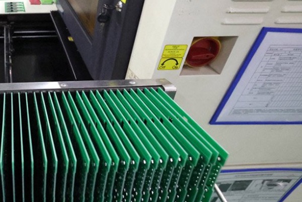
As electronic products become smaller, denser, faster, and more complex, a single inspection method is rarely sufficient. The most effective approach is to build a testing strategy around the actual PCB design, production volume, application environment, reliability requirements, and customer specifications.
As an experienced PCB manufacturing and PCB assembly service provider, Kingda supports customers from PCB prototype manufacturing and rapid PCB prototyping to PCB assembly, inspection, testing, small-batch production, and volume manufacturing.
By integrating engineering support, PCB fabrication, component sourcing, assembly, quality inspection, and testing into one manufacturing workflow, Kingda helps customers identify potential problems earlier, improve production consistency, and build reliable electronic products from prototype to mass production.