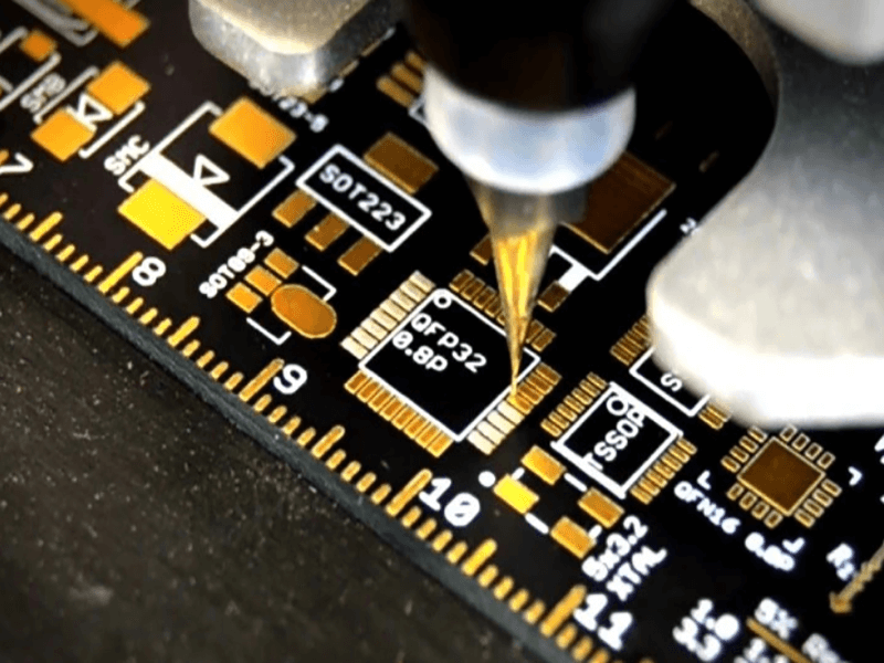
PCB Annular Ring Design And Tolerance
The annular ring is the width of copper that remains around a drilled hole after the barrel has been plated. It is the feature that connects the barrel to the trace, and it is consumed by every tolerance in the process, from the drill tolerance to the movement of the laminate during lamination. A design that specifies a pad without allowing for those tolerances produces boards with a thin or broken ring.
This article explains what eats the ring, how to calculate a minimum pad, and where a partial ring is acceptable.
What The Ring Is And Why It Matters
The ring is what carries the current from the trace into the barrel and what holds the barrel mechanically to the pad. A ring that is too thin in one place raises the resistance of the connection and reduces the strength, and a ring that disappears entirely means the barrel is connected only by the plating that survived, which is a marginal connection that may fail under thermal cycling.
The requirement is stated as a minimum remaining width at the worst case position, not as an average, because the ring is not uniform. The hole is not perfectly centred and the pad is not perfectly round, so the ring has a wide side and a narrow side, and the narrow side is what the specification applies to.

What Consumes The Ring
Four tolerances combine. The drill has a tolerance on its position and on its diameter, the pad has a tolerance on its position and on its etched size, the laminate moves during lamination so the inner layer features shift relative to the outer, and the plating reduces the hole diameter while adding to the pad. Each contributes independently, and their sum is what has to be covered by the ring.
The registration allowance is usually the largest single term. It is the misalignment between the drilled hole and the inner layer pattern, and it is quoted by the fabricator for a given stack and board thickness. A thin board with few layers registers better than a thick board with many, which is why the same pad size can be generous on one design and marginal on another.
Calculating A Minimum Pad
The minimum pad diameter is the sum of the maximum finished hole diameter and twice the required ring width plus twice the registration allowance. Taking the fabricated values rather than the nominal ones is what makes the calculation meaningful, since the finished hole is larger than the drill after plating and the pad is smaller than the artwork after etching.
The etch factor deserves its own term, because a small pad etches with more relative reduction than a large one. The fabricator can supply the etch allowance for the copper thickness in use, and it should be included rather than assumed. A pad calculated from the artwork dimensions and the drill alone will be smaller on the finished board than the designer intended.
Breakout And Its Acceptance
A breakout is a pad in which the hole is not fully surrounded by copper, so the ring is open on one side. It occurs when the tolerances are not covered, and it appears on a small fraction of the holes even in a well controlled process. Standards distinguish between a breakout that leaves the barrel connected and one that does not, and different acceptance classes treat them differently.
For a general purpose product a small breakout on a non critical net is often accepted, while the same breakout on a high reliability product is a reject. The distinction matters because the requirement affects the pad size and therefore the routing density: a design that allows no breakouts needs larger pads and consumes more board area.
Layer Dependent Differences
The ring on an inner layer is defined by the pad etched on that layer, and the registration between the hole and the inner layer pads is the critical term. The ring on the outer layer is defined by the surface pad and is affected by the plating, which adds copper and tends to enlarge the pad slightly.
Inner layer pads are therefore often specified larger than surface pads for the same hole, particularly on the layers furthest from the centre of the stack, because the movement accumulates with distance. The stack construction and the layer count determine how much movement to expect, and the fabricator can supply the registration figure for a specific construction. The stack design itself is described for layer stack up and for multilayer prototypes.
Specifying It For A Design
The design rules should state the minimum ring for each class of hole, and the fabricator should confirm the registration that the rule assumes. A rule that is copied from a previous design without checking the stack and the fabricator can produce a board that fails the acceptance criteria even though the artwork is unchanged.
The pad size also interacts with the escape routing, because a larger pad reduces the space between the pads and therefore the number of traces that can pass between them. The trade is described for escape routing, and the pad geometry itself belongs to the general rules for pad design. Where the density forces a small pad, the answer is usually a reduction in the hole size or an additional routing layer rather than a reduction in the ring.
Process Control and Verification
On a design of this kind, pad size is the item that decides how the rest of the board is arranged. Where the requirement is not written down, the shop supplies its own default, and the default is chosen for the process rather than for the design. The measurements that matter are the repeatable ones: conductor width and spacing, annular ring, finished hole size, plating thickness and surface finish are all verifiable on a coupon that travels with the panel.
Running a first article through the same checks as the production panel confirms that the two agree, and that comparison is the cheapest form of process control available at prototype stage.
Process Control and Verification
On a design of this kind, pad size is the item that decides how the rest of the board is arranged. Where the requirement is not written down, the shop supplies its own default, and the default is chosen for the process rather than for the design. The measurements that matter are the repeatable ones: conductor width and spacing, annular ring, finished hole size, plating thickness and surface finish are all verifiable on a coupon that travels with the panel.
FAQ
Is a breakout always a reject? Not always. The acceptance depends on the class of the product and on whether the barrel remains connected. A general purpose board may accept a small breakout on a non critical net.
Why is the finished hole larger than the drill? Plating adds copper to the wall and the etching and cleaning steps remove some, so the finished diameter differs from the drill diameter. The calculation uses the finished value.
Why do inner layer pads need to be larger? Because the registration between the hole and the inner layers is worse than the registration with the outer layers, particularly on the layers furthest from the centre of the stack.