PCB High‑Temperature Deformation – Causes, Impact & Prevention Strategies
With the rapid growth of automotive electronics, industrial control, new energy systems, communication equipment, and high‑power electronics, PCBs must not only meet electrical performance requirements but also provide excellent mechanical stability and heat resistance. However, during PCB manufacturing, SMT assembly, and actual operation, high‑temperature deformation has become a critical issue affecting product reliability.
Warpage, bowing, or twisting under heat can reduce placement accuracy, leading to soldering defects, BGA failures, and open circuits. Understanding the mechanisms and prevention of high‑temperature deformation is essential for improving yield and long‑term reliability.
1. What Is PCB High‑Temperature Deformation?
PCB high‑temperature deformation refers to shape changes caused by internal stress release or differential thermal expansion when the board is heated. Common forms include bow, twist, local bulging, delamination‑induced warpage, and stress‑related distortion.
Deformation can occur during lamination, electroless copper/plating, HASL, SMT reflow, wave soldering, and high‑temperature operation. It is especially prominent in multilayer, heavy‑copper, large‑size, and high‑frequency PCBs.
2. Why Does High Temperature Cause PCB Deformation?
PCBs consist of copper foil, resin, glass fiber, and other materials, each with different coefficients of thermal expansion (CTE):
- Copper: 16–18 ppm/°C
- FR4 substrate: 14–70 ppm/°C
- Polyimide: 20–40 ppm/°C
- Ceramic: 6–8 ppm/°C
During heating and cooling cycles, copper expands at a different rate than the substrate, layers heat unevenly, and internal thermal stresses build up. When these stresses exceed the board’s structural limits, warpage occurs.
Typical high‑temperature process temperatures:
- Lead‑free reflow: 245–260°C
- Wave soldering: 240–260°C
- HASL: 250–270°C
- Burn‑in testing: 125–200°C
3. Main Causes of PCB High‑Temperature Deformation
3.1 Uneven Copper Distribution
This is one of the most common causes. Large copper pours on one side, mismatched power/ground planes, or concentrated copper areas cause different expansion rates, resulting in bending moments.
Solutions: keep copper layers symmetrical, add copper thieving, and balance copper areas.
3.2 Unbalanced Stack‑up Design
Asymmetric layer stacks create unbalanced thermal stress between the top and bottom halves. A symmetric stack‑up significantly reduces deformation risk.
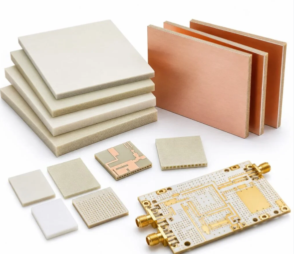
3.3 Low Tg Material
Tg (glass transition temperature) indicates heat resistance. When temperature exceeds Tg, the resin softens and rigidity drops, making permanent deformation more likely.
- Standard FR4: 130–140°C
- Mid‑Tg FR4: 150–170°C
- High‑Tg FR4: 170–200°C
- Polyimide: >250°C
3.4 Non‑Uniform Board Thickness
Uneven prepreg distribution, lamination thickness variations, or plating non‑uniformity can cause local stress concentrations and warpage.
3.5 Moisture Absorption
FR4 absorbs moisture from the environment. During reflow, trapped moisture rapidly vaporises, creating internal pressure that can cause delamination, popcorning, and deformation. Pre‑baking is essential.
3.6 Inadequate Lamination Process Control
Residual stress from lamination – affected by pressure, heating/cooling rates, and resin flow – can cause warpage even if the board is flat at delivery.
4. Impact of Deformation on Electronic Products
- Reduced SMT placement accuracy: nozzle positioning errors, component shift, uneven paste printing, and soldering defects (opens, bridges, head‑in‑pillow), especially for BGA/QFN packages.
- Lower reliability: thermal cycling may lead to solder joint cracking, intermittent failures, and field returns.
- Increased manufacturing cost: lower yield, higher rework, and reduced throughput.
5. Industry Standards for PCB Warpage
IPC standards are widely adopted:
- SMT boards: ≤0.75%
- Non‑SMT boards: ≤1.5%
- For high‑density BGA products, many customers require ≤0.5%.
Relevant standards: IPC‑TM‑650, IPC‑6012, and customer‑specific requirements.
6. Prevention in the PCB Design Phase
- Symmetric stack‑up: mirror the top and bottom halves.
- Balanced copper: use uniform copper pours, add thieving, and design symmetrical power/ground planes.
- Choose high‑Tg materials: for high‑temperature applications, select Tg ≥170°C and low Z‑axis CTE.
- Appropriate board thickness: 1.6 mm for general products, 2.0 mm+ for large boards, and add stiffeners for ultra‑thin boards.
- Avoid large empty areas: reduce local thermal expansion mismatch.
7. Process Measures to Reduce Deformation
- Precise lamination: vacuum, staged heating, slow cooling, and stress‑relief baking.
- Automated copper balancing via CAM engineering.
- Strict thickness control for dielectric and copper layers.
- AOI and flatness inspection before shipment.
8. Material Selection for High‑Temperature Environments
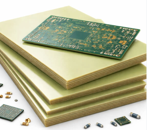
- Standard FR4: moderate heat resistance and warpage control.
- High‑Tg FR4: good heat resistance and excellent dimensional stability.
- Polyimide: very high heat resistance and flexibility.
- Rogers high‑frequency: excellent for high‑frequency and high‑temperature.
- Ceramic: superior thermal stability and minimal deformation.
Common applications: automotive radar, BMS, industrial automation, aerospace, and high‑power supplies.
9. Deformation Inspection and Test Methods
- Flatness inspection: granite platform, laser profilometry.
- Thermal cycling tests: simulate long‑term temperature variations.
- Shadow Moiré: high‑precision warpage analysis technique.
- X‑Ray: used for BGA solder joint and deformation verification.
10. Cost Analysis for Low‑Deformation PCBs
Factors influencing cost: high‑Tg materials, multilayer complexity, special lamination, flatness control, and reliability testing.
- Standard FR4 prototype: $20–80
- High‑Tg PCB: $50–200
- 6–8 layer PCB: $150–500
- High‑reliability PCB: $300–1500+
11. Why Choose gopcb for Low‑Warpage PCBs
gopcb specialises in high‑reliability PCB manufacturing with extensive experience in controlling high‑temperature deformation.
- High‑Tg and low‑CTE material systems
- Precision multilayer lamination technology
- IPC‑compliant quality control
- Full AOI and X‑Ray inspection
- Automated copper balancing optimisation
- Strict warpage control standards
Our products are widely used in automotive, industrial, telecom, medical, and new energy systems – helping customers reduce thermal deformation risks and improve long‑term reliability.
Explore our PCB manufacturing and design & layout services, or check our prototype assembly and turnkey assembly solutions.
12. Frequently Asked Questions
Q1: What is an acceptable warpage level for PCBs?
Per IPC standards, ≤0.75% for SMT boards; high‑end products often require ≤0.5%.
Q2: Does lead‑free reflow increase the risk of deformation?
Yes. Higher peak temperatures (above 245°C) create greater thermal stress, making warpage more likely.
Q3: Which PCB material is least prone to high‑temperature deformation?
Ceramic and polyimide PCBs offer the best dimensional stability and heat resistance.
Q4: Are multilayer PCBs more susceptible to warpage?
Yes, especially if the stack‑up is asymmetric or copper distribution is unbalanced. Proper design can mitigate this.
Q5: How can I reduce warpage after reflow?
Optimise stack‑up symmetry, balance copper, use high‑Tg materials, and improve lamination process control.
13. Conclusion
PCB high‑temperature deformation is a critical factor affecting manufacturing yield and long‑term reliability. Uneven copper, insufficient Tg, poor stack‑up design, moisture absorption, and residual stress are primary contributors. Through thoughtful design, proper material selection, and advanced process control, the risk of thermal deformation can be significantly reduced.
As a professional PCB manufacturer, gopcb provides low‑warpage, high‑stability PCBs for automotive, industrial, new energy, and other high‑reliability applications – helping you achieve robust product performance.