PCB Prototype Inspection and Safe Board Testing
A bare board can be perfect in the fabrication report and still fail in the lab because of how it was handled. Equally, a board with a genuine defect can pass unnoticed because the inspection was limited to a quick visual glance. Incoming inspection and safe testing practice are two halves of the same discipline, and both are cheaper than the rework that follows when they are skipped.
What Incoming Inspection Should Cover
PCB prototype inspection begins with a comparison against the drawing, before the board is used for anything else. The useful checks are dimensional and electrical: the outline and hole positions against the mechanical drawing, the copper thickness and the surface finish against the specification, and the insulation and continuity of the nets against the netlist. A board whose impedance or plating is out of tolerance will produce problems later that are far harder to trace than a rejection at goods-in.
Appearance is a legitimate part of the check, and it should be recorded rather than judged by impression. Warpage, discoloration, scratches, poor mask adhesion and marks left by handling are all visible indicators of process problems. The applicable board quality characteristics describe which of them matter and how they are measured.
Visual and Dimensional Checks
The checks that catch most problems are simple. Measure the board thickness and compare it with the stackup. Look at the soldering appearance on any pre-tinned areas, and at the flatness of the surface finish. Check the line width and spacing in a fine-pitch region under magnification, and look for residual copper or debris between conductors. Verify that the hole sizes and positions match the drawing, particularly for connectors and press-fit parts.
Colour and gloss deserve a mention because they are easy to standardise. A mask that is uneven in colour may indicate an inconsistent cure, and an unusually glossy or matt surface can indicate that the finish or the process has changed. Neither is automatically a defect, but both are worth recording when a batch is compared with a known-good reference.

Once the board passes inspection, the way it is handled during test determines whether it stays that way.
Handling and Probe Discipline
The most common way to damage a board during testing is with the probe. Multimeter leads and oscilloscope probes slip, and a slip between two adjacent pins of a fine-pitch package creates a short that can destroy the device the moment power is applied. Using fine-tip probes, keeping the board supported, and cutting power before moving a probe are basic habits that prevent most of these failures.
Soldering irons used for rework introduce a second risk. The tip must be at the correct temperature and the iron must be properly earthed; a leaky or ungrounded iron can damage sensitive devices through the tip. Where the design includes devices that are sensitive to static discharge, the workstation, the mat and the operator should all be grounded, and the protection provided by the board layout is a second line of defence rather than a replacement for handling discipline.
Powering Up a Board Safely
The first power-up is the moment when the highest risk and the least information coincide. A current limited supply, with the limit set low, tells the designer immediately whether the board is drawing more current than expected. Bringing the rails up in sequence, where the design allows it, and measuring the supply current at each step, localises a fault quickly instead of letting it spread.
Thermal checks belong in the same routine. Power components and regulators should be checked for unexpected heating within the first seconds. Where a device runs hot immediately, the cause is usually a wrong pin configuration, a solder bridge or an incorrect component value, and continuing to apply power will make the failure permanent. A thermal camera or a finger on the package – with care – is enough to catch it.
Rework Without Creating New Faults
Rework is sometimes unavoidable, and it should be treated as a controlled process rather than as a quick fix. The correct tip shape, the right flux, and a temperature that melts the joint without overheating the laminate are all prerequisites. Removing a component with too much heat damages the pad and the solder mask, and pulling the part before the solder is fully molten lifts the pad from the board.
Where a repair requires an added component or a jumper wire to bypass a damaged section, the added part should be small, and the wiring should be routed so it does not create coupling with sensitive nets. The repair should be documented with its location and its reason, because an undocumented repair is a reliability risk that nobody can evaluate later.
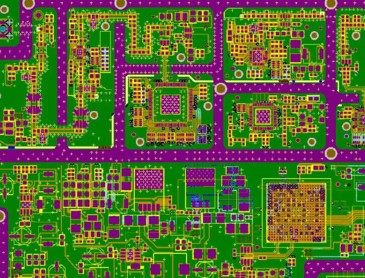
The decision to accept or reject a board should be made against defined criteria rather than against the schedule.
Recording What Was Checked
The value of inspection depends on the record it produces. A simple sheet that lists the checks performed, the measured values and the identity of the board batch turns a one-off judgement into a comparison that can be repeated. When a fault appears during functional test, the record shows whether the same parameter was already drifting, and whether other boards from the same batch are likely to share it.
Photographs are useful evidence for appearance. An image of a suspicious region, taken before any rework, preserves the appearance of the defect and answers questions that a written description cannot. Where the defect is at the limit of what the eye can resolve, a magnified image is more reliable than a judgement made at the time.
When a Board Should Be Rejected
Rejection is justified when a defect affects function, reliability or safety, and the criteria should be written down before the boards arrive. Problems on the plating, cracks or voids in the hole wall, incomplete desmear, and conductive debris between nets all fall into that category, because they may not show up until the board is in service. Cosmetic marks that do not affect the copper or the mask are usually acceptable, and rejecting them wastes both time and boards.
The distinction matters because the cost of a false rejection is real, and it is paid twice: once in the scrapped board and once in the delay while a replacement is ordered. Every board that is scrapped unnecessarily adds to the project cost and delay, while every defective board that is accepted adds risk. The manufacturability requirements behind those criteria show why the criteria should be based on the physics of the failure rather than on appearance alone.
FAQ
How much inspection is enough for a prototype batch? Enough to detect the failure modes that matter for the application: dimensional accuracy, net continuity, plating quality and cleanliness. Full qualification testing belongs with the production supplier rather than with each prototype.
Can I test a board without a current-limited supply? It is possible but unwise. A current limit turns a potentially destructive fault into a measurable reading, and it costs nothing to set.
Is rework always acceptable if the board works afterwards? No. Rework can leave a latent defect that appears under vibration or thermal cycling. It should be limited, controlled and documented, and it should be avoided in designs intended for high reliability.