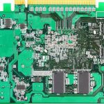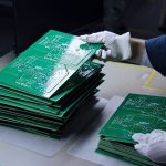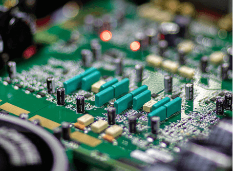
As electronic products continue to become smaller and more highly integrated, PCBA Assembly is increasingly based on Surface Mount Technology (SMT). SMT enables manufacturers to place a large number of components in a limited PCB area while supporting compact product designs, higher assembly density, and automated production.
However, many PCB designs still contain a certain number of Through-Hole Components. These components are mounted by inserting their leads through drilled holes in the PCB, making them different from surface-mounted components.
When a PCB contains both surface-mount components and through-hole components, the process is generally referred to as Mixed Assembly. In contrast, an assembly that uses only surface-mount components is considered an SMT-based assembly.
The appropriate PCB Assembly Process depends on the component types, PCB structure, component distribution, production volume, and required assembly quality. In general, PCBA production can be divided into four common configurations:
- Single-sided SMT Assembly
- Single-sided mixed assembly
- Double-sided SMT Assembly
- Double-sided mixed assembly
Understanding these assembly configurations helps engineers select an appropriate production process and optimize PCB design for manufacturability.
Single-Sided SMT Assembly
Single-sided SMT assembly means that the components are mounted on only one side of the PCB. This configuration is relatively straightforward and is commonly used when the circuit does not require components on both sides of the board.
A typical PCB Assembly Process is:
Solder Paste Printing → Component Placement → Reflow Soldering → Cleaning → Inspection → Rework
1. Solder Paste Printing
Solder paste is applied to the PCB pads through a stencil. Printing accuracy is critical because insufficient or excessive solder paste can lead to soldering defects such as insufficient solder, bridging, or component displacement.
2. Component Placement
An automated pick-and-place machine accurately places SMD components onto the printed solder paste. Component orientation, placement accuracy, feeder setup, and PCB positioning must be carefully controlled.
3. Reflow Soldering
The PCB passes through a controlled reflow profile. The solder paste melts and forms reliable solder joints between the components and PCB pads.
The reflow profile should be optimized according to the solder alloy, PCB materials, component specifications, and thermal characteristics of the assembly.
4. Inspection and Rework
After reflow, the assembly is inspected using methods such as AOI, visual inspection, and, when required, X-ray inspection. Any soldering or placement defects are repaired through controlled Rework procedures.
Single-sided SMT is relatively efficient because the PCB only needs to undergo one primary component placement and reflow sequence.
Single-Sided Mixed Assembly
Single-sided mixed assembly combines surface-mount components with Through-Hole Components, with the components located primarily on one side of the PCB.
A typical process is:
Solder Paste Printing → Component Placement → Reflow Soldering → Through-Hole Insertion → Lead Forming → Wave Soldering → Cleaning → Inspection → Rework
In this configuration, SMT components are normally processed first. After Reflow Soldering, through-hole components are inserted into their corresponding PCB holes.
Depending on the component design and production requirements, through-hole components may be soldered using Wave Soldering, selective soldering, or other suitable methods.
Key Manufacturing Considerations
The combination of SMT and through-hole assembly requires careful coordination between PCB design and production processes.
Important factors include:
- Through-hole component spacing
- Lead length and forming requirements
- Component orientation
- Solder-side clearance
- Wave soldering direction
- Thermal sensitivity of components
- PCB support during soldering
For complex mixed-technology boards, Selective Soldering may be preferred when only specific through-hole areas require soldering and wave soldering could affect nearby SMT components.
Double-Sided SMT Assembly
Double-sided SMT assembly places surface-mount components on both sides of the PCB. This approach significantly increases component density and is widely used in compact electronic products.
A typical process is:
Side A Solder Paste Printing → Component Placement → Reflow Soldering → PCB Flipping → Side B Solder Paste Printing → Component Placement → Reflow Soldering → Cleaning → Inspection → Rework
The exact sequence may vary according to component types, PCB thickness, component weight, solder paste selection, and assembly equipment.
First-Side Assembly
The first side is printed with solder paste, followed by component placement and Reflow Soldering.
Engineers should consider the thermal requirements of components and the potential effect of the second reflow cycle.
Second-Side Assembly
After the first side is completed, the PCB is flipped and the second side is processed.
Small and lightweight SMD Components generally remain attached during the second reflow because the molten solder’s surface tension can hold them in position. However, this should not be assumed for every component.
Large, heavy, or mechanically sensitive components may require special placement strategies or alternative assembly methods.
Component Placement Considerations
Component distribution between the two PCB sides should be carefully planned. Large BGA, LGA, connectors, transformers, and other heavy components can affect the second-side assembly process.
For high-density boards, engineers should also consider:
- Component-to-component clearance
- BGA and fine-pitch component placement
- Solder paste volume
- Thermal distribution
- PCB warpage
- Reflow temperature exposure
- Inspection accessibility
These considerations can significantly affect the overall PCBA Assembly yield and reliability.
Double-Sided Mixed Assembly
Double-sided mixed assembly combines SMT and through-hole components, with components distributed across both sides of the PCB.
A typical process may include:
Side A Solder Paste Printing → Component Placement → Reflow Soldering → Through-Hole Insertion → Lead Forming → PCB Flipping → Side B Adhesive Dispensing → Component Placement → Adhesive Curing → Wave or Selective Soldering → Cleaning → Inspection → Rework
The actual process should be adjusted according to the PCB design and component structure.
Adhesive Dispensing
For certain double-sided assemblies, adhesive may be applied to secure components on the PCB during subsequent processing. This is particularly useful when components on the opposite side could otherwise be affected by the assembly process.
The adhesive type, dispensing position, curing temperature, and curing time must be controlled to prevent contamination or interference with solder joints.
Wave and Selective Soldering
Through-hole components can be soldered after SMT assembly. Wave Soldering is suitable for boards with a relatively large number of compatible through-hole solder joints, while selective soldering provides more localized control for complex mixed-technology assemblies.
For high-density boards, selective soldering can help reduce unwanted thermal exposure and minimize the risk of affecting nearby SMT components.
Key Factors in PCBA Assembly Process Selection
Selecting the appropriate PCB Assembly Process requires more than simply determining whether the PCB is single-sided or double-sided.
Several factors should be evaluated during the engineering stage.
1. Component Types
The ratio of SMD components to through-hole components directly affects the assembly process. Components with special mechanical, electrical, or thermal requirements may require dedicated processes.
2. PCB Structure
PCB thickness, layer count, copper distribution, pad design, via structure, and board dimensions can affect assembly stability and thermal behavior.
3. Thermal Requirements
Multiple Reflow Soldering cycles may expose components and PCB materials to repeated thermal stress. Temperature-sensitive components should therefore be evaluated carefully during process development.
4. PCB Warpage
PCB Warpage can affect solder paste printing, component placement, and solder joint formation. The risk becomes more important for thin, large, or asymmetrical PCBs.
5. Solderability and Inspection
The selected soldering process must provide sufficient solder joint quality while maintaining compatibility with AOI, X-ray inspection, and other quality-control methods.
6. Manufacturing Efficiency
For mass production, the assembly process should balance product quality, production speed, equipment utilization, material consumption, and overall manufacturing cost.
Designing PCBs for Better Assembly
A reliable PCBA Assembly process begins with proper PCB design.
Design engineers should consider the manufacturing process during PCB layout rather than treating assembly as a separate stage.
Recommended practices include:
- Maintain adequate component spacing.
- Optimize pad and stencil designs.
- Consider the direction of wave or selective soldering.
- Avoid unnecessary thermal imbalance.
- Place heavy components carefully.
- Consider BGA and fine-pitch component inspection requirements.
- Provide sufficient clearance for assembly and rework.
- Minimize unnecessary assembly process steps.
- Evaluate PCB warpage risks for thin and large boards.
- Ensure component specifications are compatible with the selected reflow profile.
Designing with manufacturing constraints in mind can improve production yield and reduce the need for costly modifications after the PCB enters production.
Kingda’s Approach to PCBA Assembly
At Kingda, PCBA production is approached as an integrated process covering PCB design considerations, component placement, SMT assembly, through-hole processing, soldering, inspection, and quality control.
For complex assemblies, the production strategy should be determined according to the actual PCB structure and component requirements. Factors such as component density, board thickness, thermal sensitivity, soldering method, inspection requirements, and expected production volume should be evaluated before mass production.
Through appropriate process planning and manufacturing controls, Kingda helps customers improve assembly consistency, reduce process-related defects, and achieve stable PCBA Quality.
Conclusion
The four major configurations—single-sided SMT, single-sided mixed assembly, double-sided SMT, and double-sided mixed assembly—provide flexible solutions for different PCB designs and electronic products.
As electronic products continue to move toward miniaturization and higher integration, selecting the right PCBA Assembly strategy becomes increasingly important. SMT Assembly, Reflow Soldering, through-hole processing, and selective or wave soldering must be coordinated according to the PCB structure and component requirements.
By considering component placement, PCB design, thermal performance, soldering methods, PCB warpage, inspection requirements, and manufacturing efficiency at the design stage, engineers can build a more reliable and manufacturable PCB Assembly Process while improving production quality and overall product reliability.