Professional PCB Manufacturing: Technology, Quality Control, and Custom Solutions
What Is Professional PCB Manufacturing?
As electronic products become smaller, faster, and more integrated, printed circuit boards must meet increasingly demanding requirements for precision, reliability, electrical performance, and production consistency. Professional PCB Manufacturing has therefore evolved beyond basic circuit board fabrication into a comprehensive engineering and production process.
A capable PCB manufacturer needs to combine material selection, circuit fabrication, drilling, plating, lamination, inspection, and engineering support to meet the requirements of different applications. Industrial control equipment, medical electronics, automotive systems, telecommunications, computing hardware, and other advanced products may require different combinations of materials, layer counts, copper thicknesses, impedance requirements, and manufacturing processes.
Professional production also needs to accommodate different order volumes. Prototype projects may require rapid engineering feedback and flexible production, while volume manufacturing requires highly repeatable processes, stable yields, and efficient production management.
For customers looking for an integrated production solution, PCB Manufacturing can provide the fabrication foundation required before component assembly and final product testing.
1. Advanced PCB Technology and Engineering Development
The technical capability of a PCB manufacturer directly influences its ability to handle complex board designs.
Rather than relying only on standardized manufacturing processes, experienced manufacturers develop process solutions around the electrical, mechanical, and environmental requirements of each application.
High-Layer-Count and Fine-Line PCB Technology
High-layer-count boards require precise control of the stack-up, lamination process, and layer-to-layer registration.
As the number of layers increases, manufacturing challenges can include:
- Layer registration errors
- Lamination deformation
- Resin flow variation
- Interlayer connection problems
- Fine-line fabrication difficulties
- Increased drilling complexity
Manufacturers can improve production consistency by optimizing prepreg selection, lamination temperature and pressure profiles, copper distribution, and registration methods.
Fine-line circuit fabrication also requires accurate imaging and etching control. Technologies such as laser direct imaging can help improve pattern definition for high-density circuit designs.
Special Materials and Process Adaptation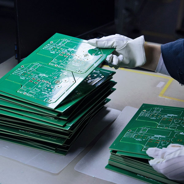
Not every PCB can be manufactured using the same material and process parameters.
High-frequency applications may require specialized laminates with controlled dielectric characteristics. High-temperature environments may require materials with improved thermal stability. High-current applications may require thicker copper structures to support current carrying and heat dissipation requirements.
A professional manufacturer should therefore evaluate material properties and adjust drilling, imaging, plating, lamination, and surface-treatment parameters accordingly.
Environmental Manufacturing
Modern PCB production also places increasing emphasis on environmental management.
Manufacturing processes may incorporate lead-free materials, halogen-reduced or halogen-free materials where required, chemical management systems, wastewater treatment, and recycling processes.
Environmental considerations should be integrated into production planning without compromising electrical performance or long-term PCB reliability.
2. Full-Process PCB Manufacturing Control
The key to reliable PCB Fabrication is not a single manufacturing step but consistent control throughout the entire production flow.
A typical process includes:
- Engineering review
- Material preparation
- Inner-layer fabrication
- Layer imaging and etching
- Drilling
- Hole preparation
- Copper plating
- Lamination
- Outer-layer fabrication
- Solder mask application
- Surface finishing
- Electrical testing
- Final inspection
- Packaging and shipment
Each stage affects subsequent processes, making process consistency essential.
Material Selection and Incoming Inspection
The manufacturing process begins with the selection and verification of raw materials.
Depending on the application, manufacturers may evaluate:
- Laminate type
- Copper foil thickness
- Dielectric properties
- Thermal characteristics
- Prepreg thickness
- Resin content
- Solder mask materials
- Surface-finish chemicals
Incoming materials should be checked against the production specification before being released to manufacturing.
Controlling material quality at the beginning helps prevent defects from propagating through later processes.
Imaging and Etching Control
Circuit patterns must be transferred accurately from the design data to the PCB material.
During imaging, important parameters include pattern dimensions, registration accuracy, exposure conditions, and surface cleanliness.
Etching must remove unwanted copper while maintaining the required trace width and spacing. Excessive etching can reduce trace width, while insufficient etching may leave unwanted copper and create electrical shorts.
For dense circuit designs, these parameters require close monitoring.
3. Precision Drilling and Hole Quality
Drilling is one of the most important processes in PCB fabrication because vias and plated through-holes provide electrical connections between conductive layers.
Mechanical drilling is commonly used for standard through-holes, while laser drilling can be applied to smaller microvias and high-density interconnect structures.
Drill Position Accuracy
The drilling system must maintain accurate hole positioning relative to the PCB artwork.
Potential causes of hole-position errors include:
- Material movement
- Tool wear
- Machine vibration
- Incorrect drilling parameters
- Thermal expansion
- Improper registration
Manufacturers can reduce these risks through tooling control, machine calibration, visual positioning systems, and process monitoring.
Hole-Wall Quality
After drilling, the hole walls must be properly prepared before copper plating.
Resin residues and drilling debris can interfere with copper adhesion and create reliability problems. Desmear and cleaning processes are therefore important for establishing a suitable surface for metallization.
For demanding multilayer boards, hole-wall quality directly affects interlayer electrical connectivity and long-term reliability.
4. Copper Plating and Electrical Reliability
Copper plating creates the conductive pathways required to connect PCB layers.
The process typically begins with electroless copper deposition, followed by electroplating to increase copper thickness.
Electroless Copper
Because the laminate and drilled hole walls are initially non-conductive, a thin conductive copper layer must first be deposited chemically.
The process requires careful control of:
- Chemical concentration
- Temperature
- Processing time
- Surface activation
- Solution condition
- Copper coverage
Uniform deposition is important for achieving reliable subsequent electroplating.
Copper Electroplating
Electroplating increases the copper thickness of the hole walls and PCB surfaces.
Current density, plating time, bath chemistry, agitation, and solution circulation all affect plating uniformity.
Poor control can result in insufficient hole-wall copper, uneven thickness, voids, or other defects that may reduce electrical reliability.
For boards with heavy copper requirements, the plating process must be adapted to the specified copper thickness and current-carrying requirements.
5. Process Traceability and Data Management
An effective PCB Quality Control system should not depend entirely on final inspection.
Process traceability allows manufacturers to associate production data with individual PCB lots or production units.
Relevant information may include:
- Material batch information
- Production equipment
- Process parameters
- Operator or production station
- Inspection results
- Electrical test results
- Final acceptance status
If a defect is discovered, traceability makes it easier to identify where the problem occurred and determine whether similar products may be affected.
Production data can also be used to identify recurring process variations and improve manufacturing parameters.
6. Comprehensive PCB Quality Control
High-quality PCB production requires multiple inspection methods because no single inspection technology can identify every type of defect.
Electrical Testing
Electrical testing verifies whether the fabricated circuit has the required electrical connections.
Typical tests include:
- Continuity testing
- Insulation testing
- Open-circuit detection
- Short-circuit detection
- Net-to-net verification
Flying-probe testing is often suitable for prototypes and lower-volume production because it does not require a dedicated test fixture.
For larger production volumes, fixture-based testing can provide higher testing efficiency.
Automated Optical Inspection
AOI systems inspect PCB patterns using optical imaging technology.
AOI can identify defects such as:
- Missing traces
- Excess copper
- Pattern abnormalities
- Pad defects
- Trace-width deviations
- Registration issues
AOI is particularly useful for detecting manufacturing defects before they move into subsequent production stages.
Microscopic and Cross-Section Inspection
For critical PCB structures, microscopic inspection can provide additional information about manufacturing quality.
Cross-section analysis can be used to examine:
- Plated hole-wall copper
- Layer alignment
- Dielectric thickness
- Copper thickness
- Lamination quality
- Via structures
This type of analysis is especially valuable for validating complex manufacturing processes.
7. Reliability Testing for Demanding Applications
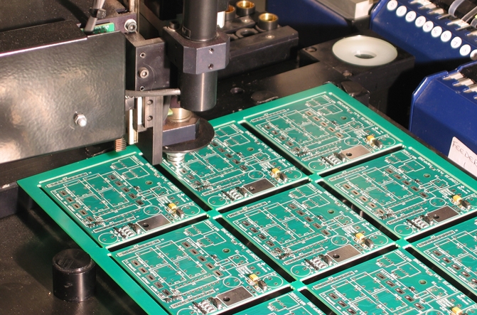
PCB reliability is not determined only by whether a board passes an electrical test immediately after production.
For demanding applications, manufacturers may need to evaluate the board under conditions that simulate its expected operating environment.
Depending on the application, reliability evaluation may involve:
- Thermal cycling
- Thermal stress
- Humidity exposure
- Solderability testing
- Copper adhesion evaluation
- Plated-through-hole reliability
- Dimensional stability testing
The exact testing program should be determined by the PCB design, materials, application environment, and customer requirements.
8. Engineering Support for Custom PCB Manufacturing
Custom PCB Manufacturing requires closer engineering coordination than standardized board production.
A manufacturing partner should ideally review the design before fabrication to identify potential production risks.
Design for Manufacturability
Design-for-manufacturing review may examine:
- Minimum trace width
- Minimum spacing
- Hole diameter
- Aspect ratio
- Pad dimensions
- Copper distribution
- Layer stack-up
- Board thickness
- Impedance requirements
- Surface finish
- Panelization
Early identification of these issues can reduce manufacturing delays and unnecessary redesigns.
For customers developing new electronic products, PCB Design and Layout support can help connect the design stage with practical manufacturing requirements.
Prototype Engineering Support
Prototype production often requires rapid engineering feedback because the board may go through several design iterations before reaching production.
A structured prototype process allows engineers to verify:
- Electrical functionality
- Mechanical fit
- Component placement
- Thermal behavior
- Signal performance
- Assembly compatibility
For this stage, Prototype PCB Assembly can support functional validation after PCB fabrication.
9. Supporting Different Production Volumes
PCB production requirements vary significantly between prototypes, low-volume production, and high-volume manufacturing.
Prototype Production
Prototype production prioritizes:
- Engineering flexibility
- Fast turnaround
- Design verification
- Small quantities
- Rapid modification
Low-Volume Production
Low-volume manufacturing requires a balance between production efficiency and flexibility.
It is often used for specialized industrial equipment, medical products, professional electronics, and products with relatively limited demand.
High-Volume Manufacturing
Large-scale production places greater emphasis on:
- Process repeatability
- Production automation
- Stable yields
- Manufacturing efficiency
- Cost control
- Consistent quality
Once a product has completed engineering validation, High Volume PCB Assembly can support the transition toward larger-scale production.
10. Why Choose a Professional PCB Manufacturer?
Selecting a PCB manufacturing partner involves more than comparing unit prices.
Important factors include:
Technical Capability
The manufacturer should have the processes and equipment required for the board’s layer count, materials, trace geometry, via structures, and copper requirements.
Quality Management
A structured quality system should cover incoming materials, in-process inspection, electrical testing, final inspection, and traceability.
Engineering Communication
Effective communication between the customer and manufacturing engineering team can reduce design-related production problems.
Production Flexibility
A capable manufacturer should be able to support prototypes, low-volume orders, and larger production requirements without compromising process control.
Assembly Integration
Combining PCB fabrication with component sourcing and assembly can simplify the supply chain and reduce coordination between multiple suppliers.
For projects requiring a complete electronics production workflow, Turnkey PCB Assembly can integrate PCB assembly, component procurement, and manufacturing coordination into a more streamlined process.
11. How to Improve PCB Manufacturing Efficiency and Yield
Manufacturers can improve production performance through several approaches:
- Standardize critical manufacturing parameters.
- Monitor raw-material quality before production.
- Maintain and calibrate production equipment regularly.
- Monitor drilling-tool condition and process stability.
- Control plating chemistry and current density.
- Optimize lamination profiles for each material stack-up.
- Use automated inspection to detect defects early.
- Maintain complete production traceability.
- Perform engineering reviews before fabrication.
- Use production data to identify recurring process problems.
The objective is to move quality control upstream so that potential defects are prevented rather than discovered only after the finished PCB has been produced.
Professional PCB Manufacturing for Complex Electronics
As electronic products continue to become more compact and sophisticated, PCB manufacturers need to provide more than basic board fabrication.
A professional manufacturing system combines engineering development, material expertise, precision processing, process monitoring, quality inspection, traceability, and customer support.
From high-density multilayer boards and fine-line circuits to specialized materials and high-current designs, different applications require different manufacturing strategies. The most effective approach is to match the PCB design, materials, process capabilities, and inspection requirements from the beginning.
Conclusion
Professional PCB Manufacturing is a comprehensive process that combines engineering expertise, advanced fabrication technology, process control, and rigorous inspection.
From material selection and circuit imaging to drilling, copper plating, lamination, surface finishing, and electrical testing, every manufacturing stage can influence the final PCB’s performance and reliability.
For companies developing new electronic products, choosing an experienced manufacturing partner can simplify the transition from prototype to production while improving quality consistency and supply-chain efficiency.
By combining reliable PCB Fabrication, structured PCB Quality Control, and flexible Custom PCB Manufacturing capabilities, Gopcba can support electronic product development across different industries and production volumes.