6G High Frequency PCB: What the New Plan Demands
On 7 September 2026 the Ministry of Industry and Information Technology published its information and communications industry plan for the fifteenth five year period, and the wording on 6G changed from research topic to commercial pathway. The plan calls for launching 6G commercial service at an appropriate time, alongside continued research into 6G key technologies, terminal development and 5G-Advanced network construction. It sets cumulative information infrastructure investment of 3.8 trillion yuan by 2030, five hundred thousand new 5G-Advanced base stations during the plan period, and intelligent computing capacity of 9,800 EFLOPS. That schedule is why 6G high frequency PCB work has to begin well before the first commercial network exists.
None of that builds a 6G network this year. What it does is commit the industry to an upgrade path in which 5G-Advanced carries the near term load and 6G follows, and that sequence determines when high frequency board requirements become commercial rather than experimental. For anyone designing radio frequency and high speed hardware, 6G high frequency PCB requirements now have a schedule attached to them.
What the Plan Actually Commits To
The distinction that matters is between technology trials and deployment. Earlier programmes concentrated on standards work and laboratory validation. This plan places 6G inside a national five year commercial framework while assigning 5G-Advanced a clear role in network construction and early verification, which means equipment makers have to design hardware now that can evolve into the later standard without a complete redesign.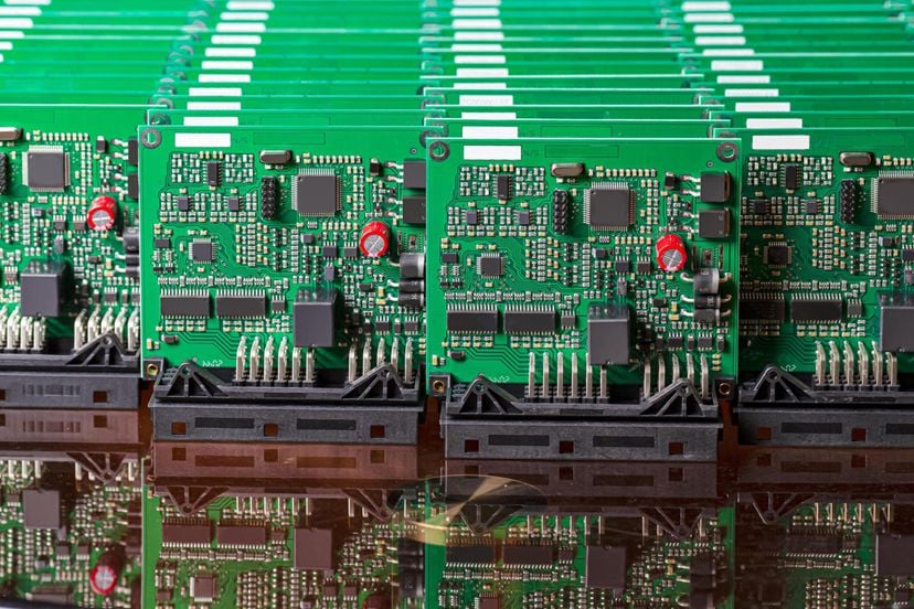
The investment figure reinforces that reading. A cumulative 3.8 trillion yuan across information infrastructure is a commitment to physical equipment, and base stations, backplanes, switching platforms and computing hardware all consume boards. When a buildout of five hundred thousand 5G-Advanced stations is specified alongside a computing capacity target, the demand signal reaches radio frequency front ends and data centre hardware at the same time.
Antenna Arrays Turn Consistency Into the Hard Problem
Massive MIMO already places many radio channels on one antenna panel, and the move toward higher frequency bands and larger arrays increases their number further. Higher frequency means signal loss along the board becomes more significant, so material dielectric loss, copper foil roughness and small dimensional deviations that were previously tolerable now consume part of a shrinking budget.
The harder requirement is phase and amplitude consistency across channels. Beamforming depends on the relationship between signals from many channels, so if trace lengths, impedances or dielectric properties differ slightly between them, the error appears as a distorted beam rather than as a fault on one line. This is a manufacturing problem before it is a design problem: reproducing the same electrical behaviour across hundreds of channels on a panel requires tight process control, and it is the reason high frequency manufacturing capability is judged on repeatability rather than on the best single measurement.
Sensing and Communication Load One Board With More Jobs
5G-Advanced is already being used to validate integrated sensing and communication, and the direction of travel is toward base stations that also perform environmental sensing, positioning and edge computing. Adding those functions changes the internal architecture of the equipment rather than only the software running on it.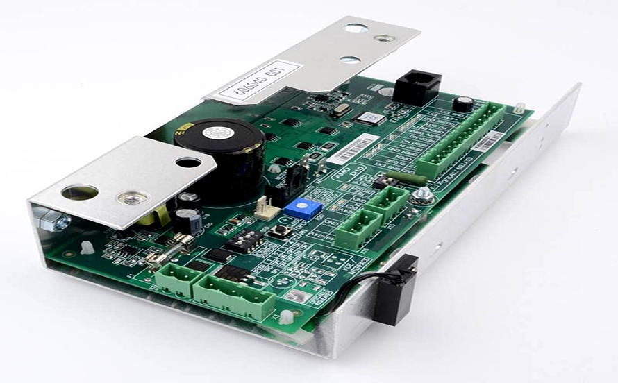
Radio frequency front ends, digital processing, power and high speed interconnect end up sharing a smaller volume, so device density rises and high layer count and HDI construction becomes normal in baseband and processing boards. Where processors, field programmable gate arrays, switch chips and high speed memory exchange large volumes of data, the board also has to support many differential pairs with continuous reference planes. Layer stack design and impedance continuity therefore become the limiting engineering tasks, not the choice of a single transceiver chip.
Materials Follow Frequency, Not Fashion
Low loss laminates are chosen because dielectric loss rises with frequency, and at the frequencies now in use the difference between a well behaved material and an ordinary one is measurable in system margin. Copper foil matters for the same reason, since conductor loss depends on surface roughness at high frequency, which is why low profile foils appear in radio frequency stack ups alongside the laminate selection.
Mixed constructions are often the practical answer: low loss material on the layers that carry radio frequency and high speed signals, with more economical grades used where the electrical requirement is lower. That approach controls cost, but it introduces process complexity, because different materials expand at different rates during lamination and their dielectric thickness behaviour under pressure is not identical. Managing that combination is a manufacturing skill, and it belongs to a factory that already runs controlled PCB manufacturing processes rather than one learning on a first article.
Impedance Control Across a Batch
Impedance depends on trace width, spacing, copper thickness, dielectric thickness, dielectric constant and the shape of the trace after etching. Controlling one trace to a target is routine. Controlling thousands of them so that the same nominal design behaves identically on every panel is a different requirement, and it is the one that communication equipment imposes.
Meeting it requires coupon measurements on production panels, feedback into the etching and lamination processes, and enough process stability that corrections are small. Designers help by keeping trace geometry within the range the factory controls well, avoiding unnecessary changes in width between layers, and specifying tolerances that reflect what the process can hold rather than what looks attractive on a drawing. Those decisions are made during layout and stack up design, and they determine how much margin remains for manufacture.
The Compute Side Adds a Second Wave of Demand
The plan also targets intelligent computing capacity of 9,800 EFLOPS by 2030, which means data centre and switching hardware expand in parallel with the radio network. High speed backplanes, switch line cards and server boards carry the same electrical challenges as radio boards but at much larger scale, with many high speed differential channels running across long distances inside a rack.
Backplanes of this class use high layer counts, thick boards and demanding impedance requirements, and they are assembled into systems where a single board failure affects an entire shelf. That combination explains why the demand from computing infrastructure is valuable to board manufacturers: volumes are large, requirements are technical, and qualification is difficult enough to reward suppliers who have invested in process control rather than in capacity alone.
Process Windows Narrow as Frequency Rises
Higher frequency makes every manufacturing variation more visible. Drilling quality and hole wall preparation affect plated barrel integrity, and at high layer counts the accumulated misregistration between layers reduces the margin available at the drill target. Multiple lamination cycles also introduce dimensional change that has to be measured and compensated rather than assumed.
Low loss materials add their own constraints. Their processing windows are narrower, they may be more sensitive to moisture before lamination, and they behave differently when mixed with standard grades in one stack up. A factory building this class of product usually has established parameters, qualified material combinations and inspection points at each stage, because the alternative is discovering a process interaction on a finished panel. That structured approach is what a defined manufacturing flow is meant to deliver.
From Prototype to Volume Without Redesign
Communication hardware development usually starts with a small number of evaluation boards, moves to field trials and then to volume. Each of those stages has a different manufacturing requirement, and the most common cause of delay is a design that cannot be built at the second stage without changing the stack up it was validated on.
Keeping the same material class, layer count and impedance targets through the transition avoids requalifying the radio performance, and it is easier when one supplier handles the prototype and the production build. Verification is the other half of the path: radio frequency assemblies need testing that reflects the parameters that matter, from impedance coupons to functional checks after assembly, and that test coverage has to survive the move to higher volume. Establishing assembly testing early makes the transition a scaling exercise rather than a redesign.
Thermal and Mechanical Loads Grow With Density
Higher integration puts more heat into less area. Radio frequency power amplifiers, processors and power conversion circuits all dissipate energy, and the board has to move that heat into the enclosure without distorting the electrical behaviour of the material. Thermal vias, copper planes and a stack up that conducts heat away from the hot spots are standard measures, but they only work if the mechanical design of the product provides a path out of the assembly.
Mechanical requirements move in the opposite direction. Dense equipment is often mounted in racks and subjected to vibration during transport and operation, so heavy components need mechanical support and connector interfaces need strain relief. On high layer count boards, a repeated thermal cycle can also act on the interface between materials, which is why reliability testing of finished assemblies matters as much as first article electrical performance.
Cost Discipline in a High Frequency Design
Radio frequency and high speed boards are expensive by nature, and cost control usually comes from disciplined use of premium material rather than from cheaper processing. Replacing control impedance specifications with measurement based limits, panelising to a size the factory handles efficiently, and avoiding unnecessary layer count all reduce price without reducing performance.
Buyers should also look at how much of the work stays inside one supplier. When drilling, lamination, plating and assembly happen under coordinated control, a process interaction is resolved internally instead of becoming a discussion between vendors, which is generally faster and cheaper than the alternative. Once a design is stable, that coordination is what turns a difficult prototype into a repeatable product.
What to Watch in 5G-Advanced First
The immediate demand indicator is not 6G itself but how quickly 5G-Advanced construction pushes technical requirements into volume production. Station counts, antenna channel counts and the introduction of sensing functions will show whether high frequency boards are moving from specialized programmes into mainstream equipment.
For board manufacturers the useful preparation is unglamorous: qualify more low loss materials, tighten impedance and registration control, and build process data that can be shown to a customer evaluating a new platform. Programs in telecommunications electronics tend to be awarded on evidence rather than on promises, and the suppliers holding that evidence when 6G volumes arrive will be the ones already producing for 5G-Advanced.