Aerospace PCB Design: Layout Rules That Keep Avionics Reliable
An aerospace PCB is asked to do something ordinary boards are never asked to do: keep working while the environment tries to destroy it. Vibration, wide temperature swings, low pressure, humidity and salt fog all act on the same assembly, and none of them can be serviced after launch. That single constraint drives every design decision, from material selection to the amount of extra copper left around a via.
The result is a board that looks familiar but is specified very differently. Tolerances tighten, derating margins widen, documentation grows, and every choice must be traceable to a requirement rather than to habit.
Start With the Environment, Not the Schematic
Design begins by writing down the environment. Expected ambient and soak temperatures, thermal cycling range, vibration spectrum, altitude, humidity and any radiation exposure determine the material set and the mechanical approach. A board that will sit in a pressurized cabin has different needs from one inside an unpressurized bay.
Only after those numbers are fixed does component selection start. Parts are chosen for rated temperature range, outgassing behavior and availability of qualification data. Where a commercial part is unavoidable, the design must show that the derated operating conditions stay inside its verified envelope.
Materials and Stackup for Flight Hardware
Standard FR-4 is often replaced or upgraded. Higher glass transition temperature laminates resist the delamination and barrel cracking that appear after repeated thermal cycles. Polyimide is used where the temperature range is widest, and ceramic-filled or low-loss materials appear where high-frequency RF performance matters.
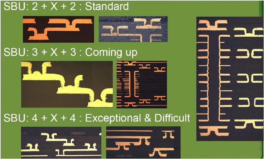
The stackup is symmetric and balanced. Copper distribution is controlled across each layer to avoid warp during lamination and to keep the board flat through thermal excursions. Layer count is set by routing and shielding needs rather than by minimum cost, and the resulting stackup is documented with dielectric thickness, prepreg style and copper weight for each layer.
Thermal Management Is the Primary Design Task
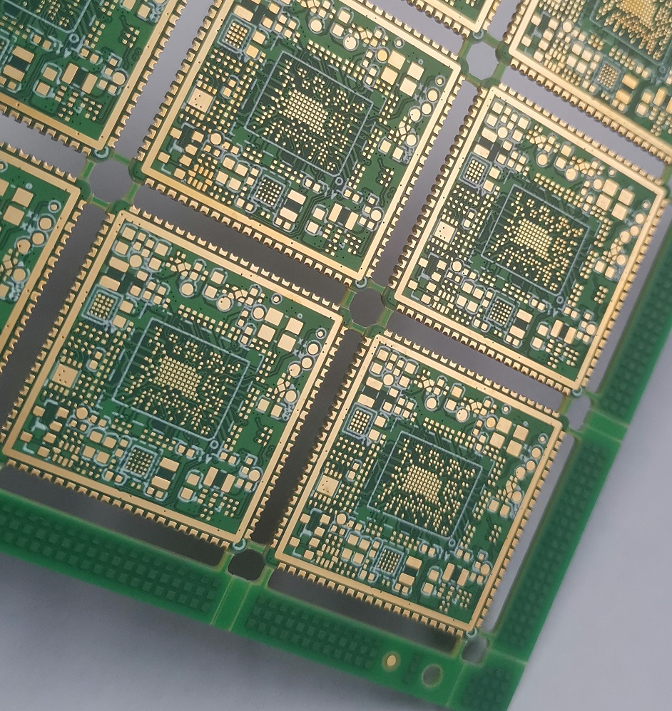
Thermal management in avionics is rarely about a single hot component. It is about moving heat out of a sealed enclosure where convection is limited. Conduction becomes the main path, so thermal vias under power devices, copper pours tied to a plane, and direct attachment to a chassis or cold plate all carry the load.
Component placement follows the thermal map. Heat-generating devices are spread rather than clustered, and temperature-sensitive parts such as oscillators and precision references are kept away from them. The board outline and mounting pattern also influence heat flow, since screws and standoffs create conduction paths to the structure.
Where cooling is marginal, the design may add metal-core sections, heavier copper, or a bonded heat spreader. Each adds mass and cost, so the thermal analysis is done early, and the result is verified by test rather than assumed from simulation.
High-Frequency RF Layout Under Vibration
High-frequency RF sections demand controlled geometry plus mechanical stability. Impedance is set by trace width, dielectric constant and reference plane spacing, and it must stay consistent along the entire path. Connector transitions are modeled rather than guessed, and ground stitching around the RF block is dense enough to keep return currents short.
Vibration adds a constraint that consumer designs ignore. Large components, tall connectors and heavy shielding cans are the first to crack a solder joint. Parts are placed close to mounting points or stiffened by a bracket, and the mass of any component is considered part of the mechanical design.
Impedance Control and Signal Integrity
Impedance control is specified on the fabrication drawing with a tolerance, typically plus or minus ten percent, and verified with test coupons on the panel. The stackup, trace width and dielectric values are agreed with the fabricator before release, because a supplier who etches slightly narrower traces will shift the impedance outside tolerance.
Differential pairs are length matched within a few mils, referenced to a continuous plane, and routed without splits under the pair. Return path continuity matters more than any single trace dimension; a plane split under a clock or RF line creates a radiating loop that no amount of shielding will fix.
Derating, Margins and the Three-Amp Rule
Current derating is where aerospace boards differ most visibly from commercial ones. A trace sized for two amps of expected load may be designed to carry three, so abnormal peaks and transients do not push the conductor toward its thermal limit. The same logic applies to voltage ratings, capacitor ripple and connector pin current.
Extra copper also lowers voltage drop and reduces temperature rise, which extends the life of every joint on the board. Wide power traces, multiple vias per connection and generous pad sizes look oversized on a schematic; they are sized against worst-case current, not nominal current.
Assembly, Coating and Documentation
Assembly notes are part of the design. Conformal coating coverage, keep-out areas for coating, staking of heavy components and the sequence of mechanical assembly are all specified. Coating protects against humidity and condensation but must not be applied to connectors or test points that need contact.
Documentation closes the loop. Fabrication notes define materials, tolerances and inspection; assembly notes define processes and acceptance criteria; and traceability records connect each board to its material lots and test results. The paperwork is not decoration. Without it, a qualified board cannot be reproduced or defended.
Screening, Qualification and Test
Components for flight hardware are often screened before assembly. Screening may include burn-in, thermal cycling and electrical test at temperature extremes, performed on the parts rather than on the finished assembly. The purpose is to remove early-life failures that would otherwise appear after the board is sealed into a chassis.
The finished assembly is then tested against the requirements it was designed for: functional test at temperature, insulation resistance, continuity and, where specified, vibration and thermal vacuum exposure. Test points and connector access must be designed in, because a board that cannot be probed cannot be qualified.
Verifying the Design Before Fabrication
Pre-layout simulation checks impedance, crosstalk and power integrity. After layout, a design review covers creepage and clearance, thermal relief, mounting tolerances and hole-to-edge distances. Mechanical drawings are cross-checked against the board outline and the enclosure model.
Prototype builds then validate the assumptions. Boards are inspected, coated and subjected to thermal cycling and vibration before the design is released. Problems found at this stage cost engineering hours; problems found after qualification cost programs.
FAQ
Can commercial-grade components be used in aerospace assemblies? Yes, when the design derates them and the operating conditions stay inside a verified envelope. The work is in documenting that envelope and proving it with test data rather than relying on the part datasheet alone.
Why do aerospace boards use so many extra vias and wider traces? Redundancy. Extra vias reduce current density and thermal stress per barrel, and wider traces lower voltage drop and temperature rise. Both extend service life under cycling, which matters when replacement is impossible.
What is the single most common aerospace layout mistake? Treating the plane as a single ground. Splitting analog, digital and power returns deliberately, then stitching them at one controlled point, prevents the noise coupling that appears later as intermittent faults in the field.
Related reading: conformal coating and board protection, via in pad versus plated through, and multilayer prototype requirements.