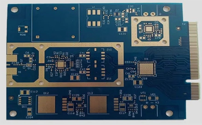
Aluminium Nitride: Design Rules and Process Limits Alumina has been the default ceramic substrate for decades because it is inexpensive, well understood and adequate for most applications. Aluminium nitride exists because alumina’s thermal conductivity is modest, and a substrate that insulates electrically while conducting heat is exactly what a power…

Thermal Via Design and Copper Spreading Under Power Devices A power device converts a fraction of its current into heat, and that heat has to leave the package through the board or through a heat sink. Where the primary path is the board, the design of the copper beneath the…
Multilayer PCB Design: Rules That Hold Up in Production A multilayer PCB is not simply a double-sided board with extra layers. The added layers are a resource that has to be allocated deliberately, and the decisions made in the first hour of layout, about size, layer count and placement, are…
Five-Order Blind Via HDI Boards: Process Flow and Control A five-order blind via board is the point at which high density interconnect stops being a variation on conventional multilayer fabrication and becomes a separate discipline. Each order of blind via adds one more sequential lamination cycle, one more laser drilling…
Copper Thickening In DPC Ceramic Substrates Direct plated copper substrates begin as a thin sputtered seed layer on a ceramic surface, which is enough to carry a circuit but not enough to carry tens of amperes. Thickening that layer by electroplating is what turns the process into one suitable for…
First Article Inspection: Design Rules and Process Limits First article inspection is the point at which the first production board is measured against the drawing rather than against expectations, and it is the cheapest opportunity in the whole program to find a discrepancy. Skipping it moves the discovery to a…
Glass Transition Temperature: PCB Laminate Properties That Affect Manufacture A printed circuit board starts as a stack of materials that have to keep their dimensions through heat, pressure and chemical processing, and the properties that make that possible are not the ones a designer normally thinks about. Understanding them explains…
Via Stub: Via Design Rules and Their Hidden Cost Vias are the least examined feature on most boards and the one that carries the most hidden cost. Each one is a hole, a plating operation and a discontinuity, and the design rules around them determine both the density that can…
Gate Driver Layout for Silicon Carbide and GaN Stages Silicon carbide and gallium nitride devices switch in a few nanoseconds, and that speed is the point of using them. It also means that every nanohenry of inductance in the gate driver path produces a voltage spike that can exceed the…
Fabrication Data Review Before Release Most problems found during fabrication originate in the front end, in the data and the instructions rather than in the process, and the cost of correcting them is paid in schedule. A short review before the data is released removes most of them. Data Completeness…