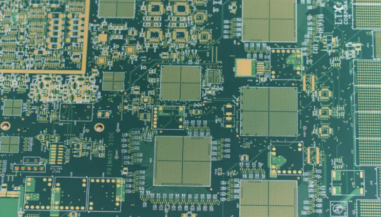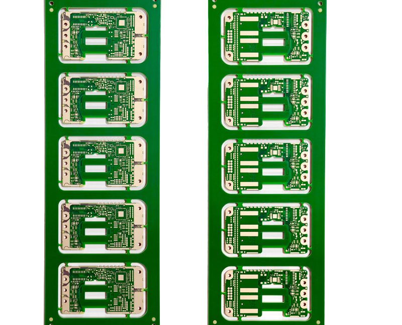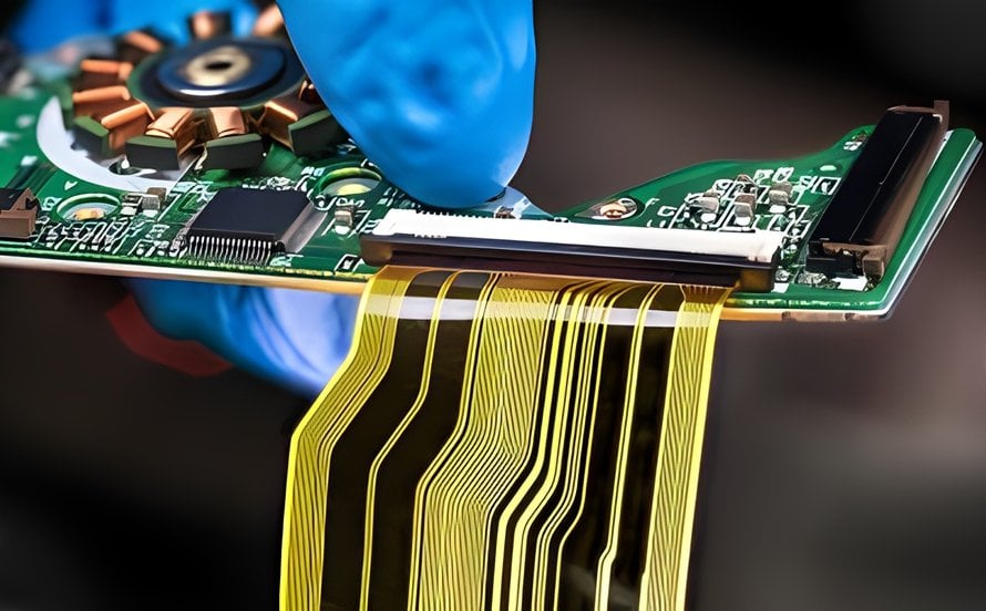
PCB Layout Planning: Structure, Placement and Routing Strategy Layout is where a correct schematic either becomes a working product or a source of problems that no amount of firmware work will fix. Most of that outcome is decided before the first track is drawn, in the decisions about board structure,…
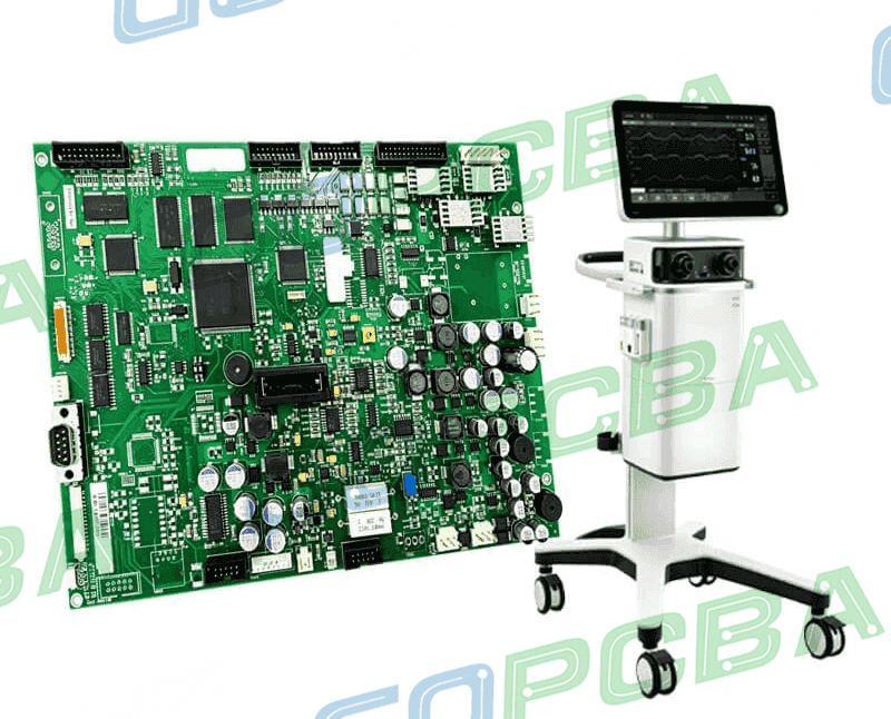
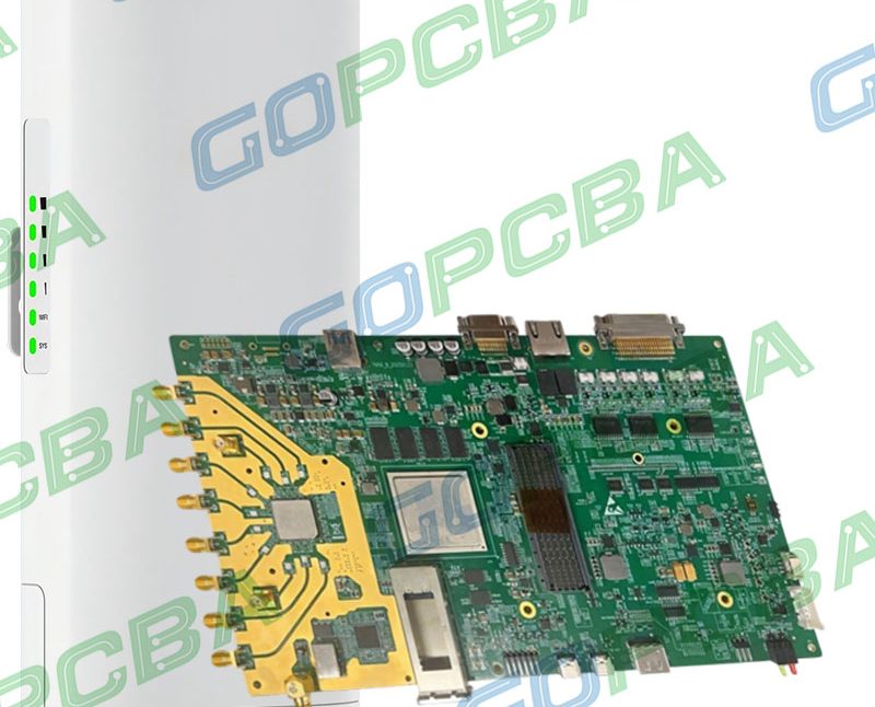
Core Board PCB Classification: Layers, Materials and Construction A core board is the small, self-contained module that carries the processor, memory and essential support circuitry, leaving the application-specific design to a larger carrier board beneath it. Because the term describes a role rather than a single product, core boards come…
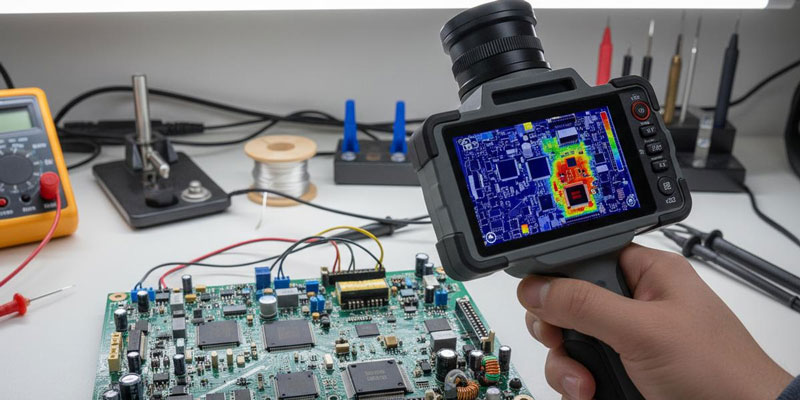
PCB Quality Control: Test Methods on the Production Floor Every process step can introduce a defect, and the defects look different depending on where they were created. That is the fundamental reason PCB quality control cannot rest on a single method. A board that passes one test may still carry…
Sizing a Plating Tank for PCB Production A plating line is sized once and then lives with the consequences for years. Too small a tank and the bath overheats during a heavy load, the chemistry drifts, and the deposit varies from panel to panel. Too large a tank and the…
Instant PCB Quote vs Traditional RFQ: Time and Cost Quoting is the first place a design meets manufacturing reality, and it is also the first place a schedule can be lost. An instant PCB quote returns a price and a lead time in seconds from an uploaded set of Gerber…
Rogers vs Taconic: Choosing a High Frequency Laminate Two laminates can share a dielectric constant and still behave very differently on the bench and on the production line. Rogers and Taconic both supply high frequency materials that engineers compare constantly, and the Rogers vs Taconic question has no single right…
PCB Trace Antenna versus Chip Antenna: Cost and RF Performance Nearly every wireless product built in the last decade has had to answer the same question, usually late in the schedule: does the antenna live on the board as copper, or does it arrive as a component? A PCB trace…
BGA Assembly versus LGA Assembly: Process and Inspection BGA and LGA packages solve the same problem in two different ways. Both put a dense array of connections on the underside of the device so that hundreds or thousands of inputs and outputs fit under a chip the size of a…
Exposed Copper on a PCB Pad: Causes and Cures Bare copper is the normal state of a pad before the finish is applied and an abnormal state almost anywhere else. When it appears where it should not, either the mask has failed, the finish has been damaged, or handling has…
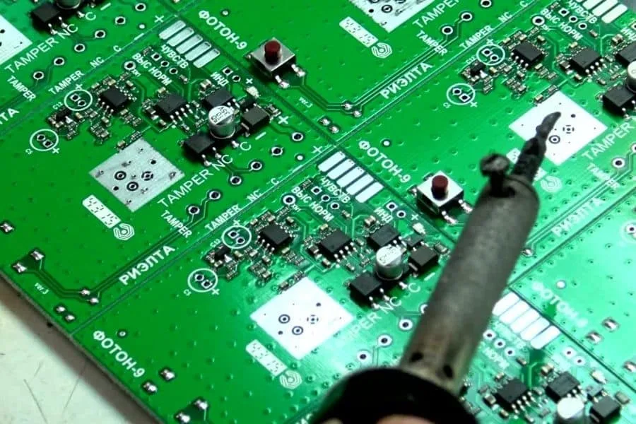
Solder Mask Misregistration: Causes and Fixes Solder mask misregistration is the mismatch between where a mask opening was designed and where it lands on the finished board. It is a small error in absolute terms, often measured in tens of micrometres, but it moves in the wrong direction on a…