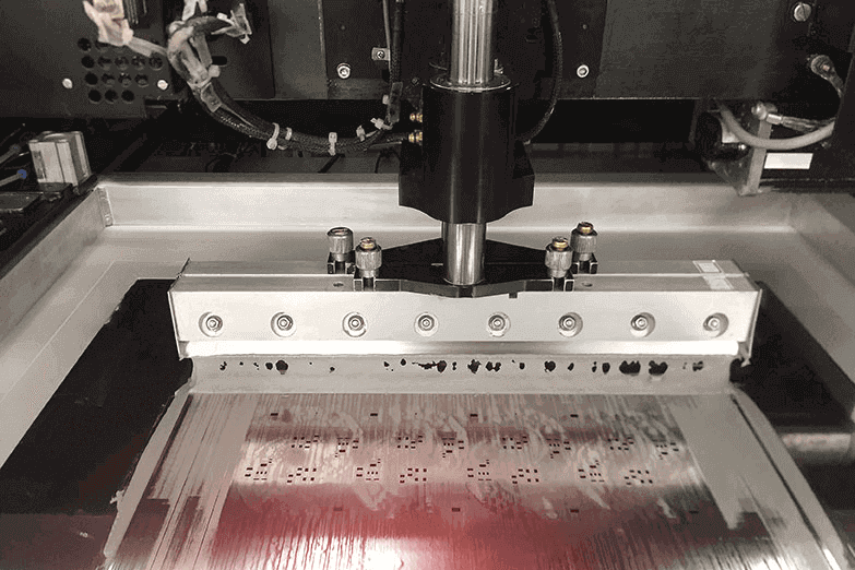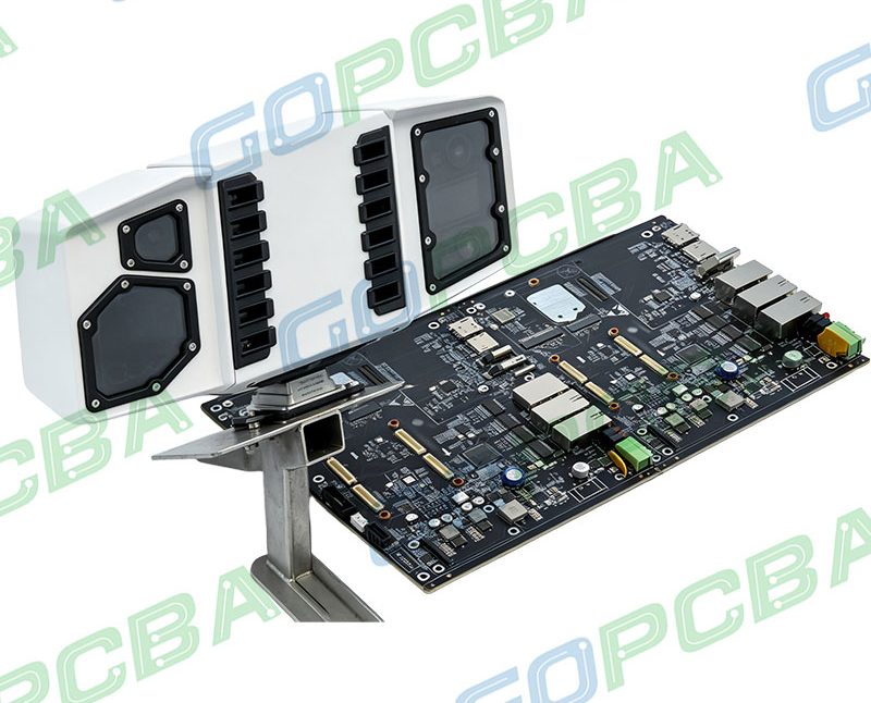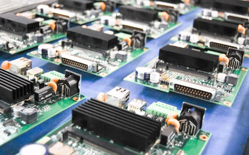
PCB Tooling Charge Explained: What the First Order Pays For Electronics manufacturing has become a discipline of small details. Solder paste volumes, placement accuracy, temperature profiles and inspection limits all add up to the final result. This guide looks at PCB tooling charge explained from the perspective of a PCBA…
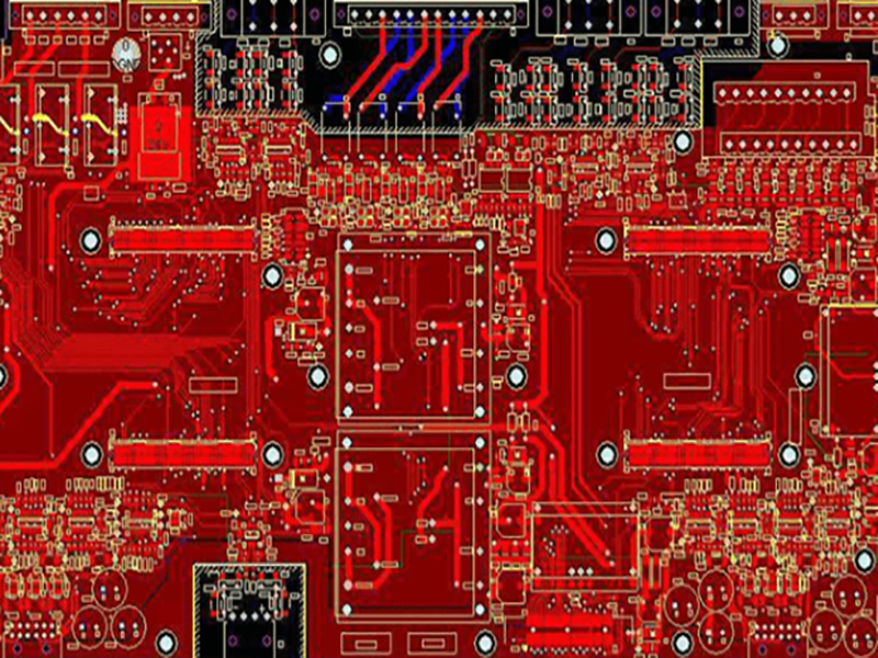
PCB Electrical Clearance and Spacing Requirements Explained Spacing is the part of a layout that nobody notices until the board fails. A trace that runs 4 mil from its neighbour is a reliability experiment, not a design; a pad that sits 0.1 mm from the board edge is a short…
Five Key Points of PCB Board Design Most of what determines whether a board is quiet, manufacturable and easy to build comes down to five decisions that are made before detailed routing begins. None of them is complicated, and all of them are easier to get right at the start…
Common PCB Design Problems That Delay Fabrication and Assembly Most boards that come back from fabrication with a query, or from assembly with an unexpected defect, are not failing because of an exotic mistake. They are failing because of a small set of familiar issues that are easy to introduce…
Electrical Test in PCB Production: Opens, Shorts and Fixtures A bare board that passes visual inspection can still contain a broken track inside a via, a short between two inner layers, or a connection that is marginal enough to fail in the field. Electrical test is the only step in…
PCB Export Crating and Palletising: Ready for the Container Electronics manufacturing has become a discipline of small details. Solder paste volumes, placement accuracy, temperature profiles and inspection limits all add up to the final result. This guide looks at PCB export crating and palletising from the perspective of a PCBA…

SMT vs Through-Hole Components for PCB Assembly Every board carries a mix of surface-mount and through-hole parts, and the split is usually decided by habit rather than by analysis. Both families are mature, and the right choice depends on which property matters most for that net: density, thermal path, mechanical…
PCB Layout Component Spacing Rules and Twelve Practical Checks Most assembly problems that reach the production line were decided months earlier on the layout screen. A part placed 0.1 mm too close to its neighbour turns a normal stencil print into a bridging defect; a thermal pad connected to a…
PCB Design Factors: Layers, Vias, Silkscreen and Pads Most layout problems trace back to a handful of concepts that are easy to use without understanding. A pad that was placed as a default, a via that was copied across the board, a copper pour that was drawn as a rectangle…
PCB Shipping Damage Claim: When the Box Arrives Broken Buyers and engineers often focus on the finished product and forget the production line behind it. In practice, most field failures can be traced back to process decisions made during assembly. Understanding PCB shipping damage claim gives you a practical advantage…