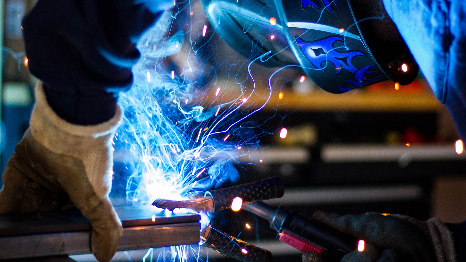
Cold Solder Joint Prevention: Flux, Tip Temperature and Pad Cleanliness Hand soldering looks simple until a board comes back from test with an intermittent connection that disappears when the probe touches it. Almost every one of those failures is a cold solder joint, or its close relative the false joint,…
PCB Desiccant and Humidity Indicator: The Warning Card Buyers and engineers often focus on the finished product and forget the production line behind it. In practice, most field failures can be traced back to process decisions made during assembly. Understanding PCB desiccant and humidity indicator gives you a practical advantage…
Signal Integrity Design for Gigabit PCB Interconnects Gigabit links moved high-speed design out of the laboratory and onto ordinary backplanes and line cards, and with that move the assumptions that had served at lower rates stopped holding. A trace that was previously treated as a wire now behaves as a…
EMC Design for Switching Power Supply PCB Layout Switching supplies are among the most demanding boards to lay out for electromagnetic compatibility, because the interference is generated by the circuit’s normal operation rather than by a fault. Currents and voltages change rapidly by design, the switching node is a small…
Component Placement: Using the Ratsnest as a Guide Component placement is often treated as the stage before the real work, and then the real work turns out to be impossible. Designers recognise the experience: a few connections remain, no path exists for them, and the only way forward is to…
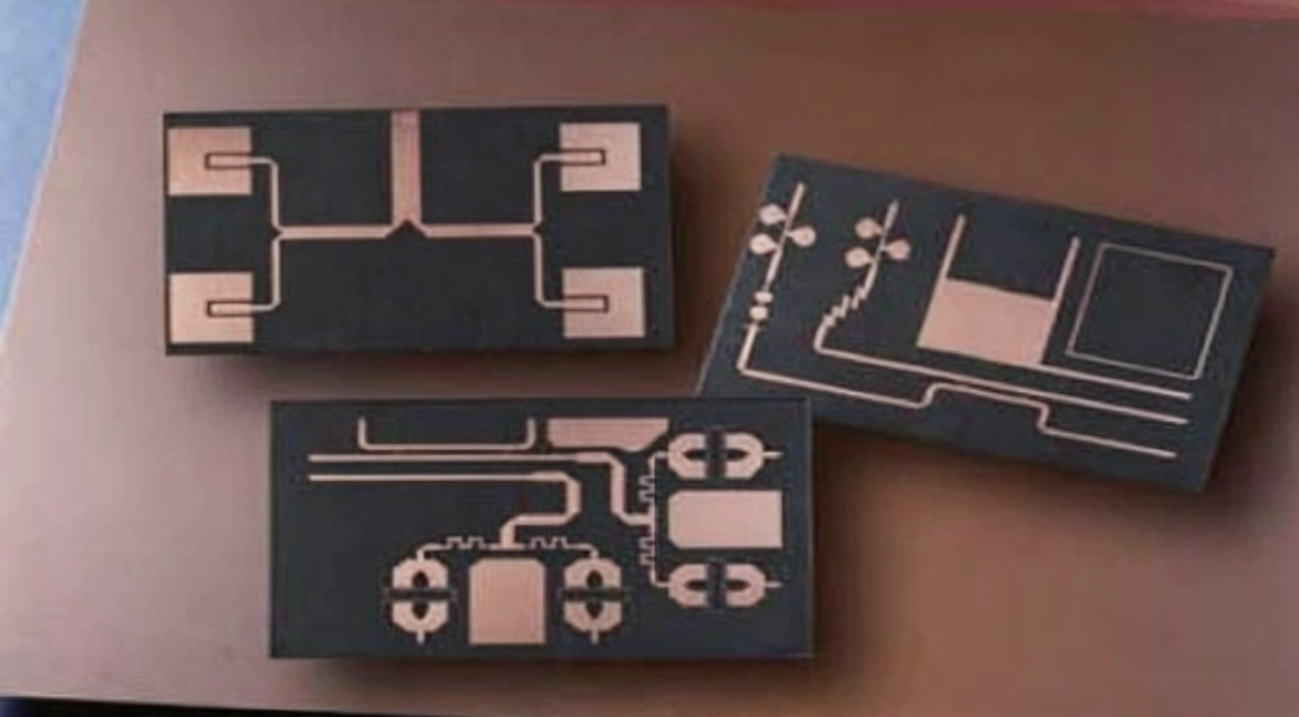
PCB Fabrication Processes: Subtractive, Additive, and Semi-Additive Every printed circuit board is produced by one of three basic strategies: material is removed to leave conductors, material is added until conductors exist, or the two approaches are combined. Which one a fabricator uses determines the achievable line width, the panel cost,…
Power Plane Inset in Multilayer Boards: Why and How Much On a multilayer board the power and ground planes are usually the largest copper features in the design, and where they stop matters. A plane that runs all the way to the board edge presents an exposed copper edge to…
SMT Micro-Assembly Technologies: MCM, Flip Chip and PoP Micro-assembly is the bridge between a finished circuit board and a working miniature product. It combines fine-pitch soldering, die-level interconnection and package stacking on a high-density interconnect substrate, and it is normally applied to small and medium production batches where a full…
PCB Substrate Defects: Blowholes, Adhesion Loss, and Dimensional Drift Most board defects are discussed in terms of copper, plating, or assembly, but a significant share originates in the base material itself. The laminate determines how the board expands with temperature, how strongly the copper adheres to it, and how much…
High-Speed Simulation Workflow for PCB Design High-speed design decisions are expensive to change late, and a high-speed simulation is the cheapest way to make them early. The practical question is not whether to simulate but what to simulate, at which stage and to what accuracy. A workflow that answers those…