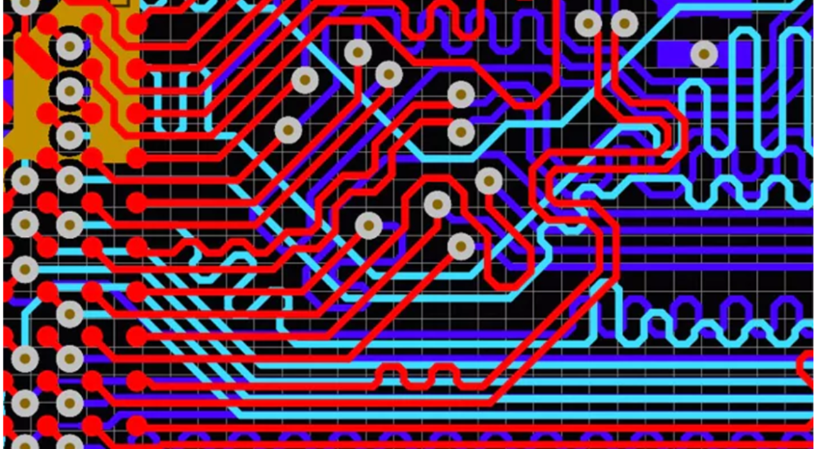
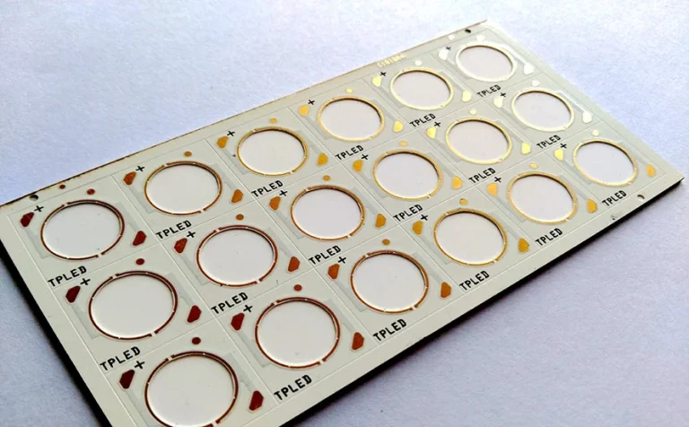
Transmission Line Types in High-Speed PCB Layout High-speed design is often described as if it starts at some magic clock frequency, but frequency is not what matters. What matters is whether the edge of the signal is fast enough and the trace long enough that the conductor behaves like a…
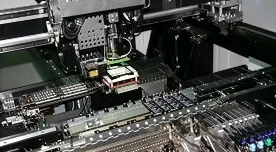
PCBA Soldering Requirements for the PCB Design Soldering does not begin at the assembly house; it begins with the board design. Heat resistance, board shape, edge clearance, fiducial marks and panelization all have to be correct before the first board reaches the paste printer. When they are not, the line…
PCB Bend and Flex Testing: How Far It Bows Buyers and engineers often focus on the finished product and forget the production line behind it. In practice, most field failures can be traced back to process decisions made during assembly. Understanding PCB bend and flex testing gives you a practical…
Plasma Treatment in PCB Fabrication: Desmear and Surface Activation Plasma treatment has moved from a specialty step to a routine one in PCB fabrication, because the surfaces that modern boards rely on, including polyimide, PTFE, filled resins and laser-drilled via walls, are chemically inert and do not wet reliably without…
12 PCB Layout Tips for Spacing, Decoupling and Teardrops Most layout problems that reach the assembly line were decided long before the file was released, and a handful of them account for the majority of rework. The PCB layout tips below cover the spacing, placement and pad decisions that affect…
PCB Drop Test for Assemblies: The First Fall Buyers and engineers often focus on the finished product and forget the production line behind it. In practice, most field failures can be traced back to process decisions made during assembly. Understanding PCB drop test for assemblies gives you a practical advantage…
Signal Routing Order: Prioritizing Nets on Dense Boards On a dense board, the order in which nets are routed matters as much as the routing itself. A clock line routed after the data bus has to detour around obstacles that the bus already occupied, and the resulting length, layer changes,…
Reading an Eye Diagram: Jitter, Noise, and Signal Quality Serial links are verified in the frequency domain with insertion loss, and in the time domain with an eye diagram. The second view is often more informative for layout work, because it shows the combined effect of every impairment in the…
PCB Laser Drilling: UV, CO2, and Hybrid Systems Compared Microvias are what make high-density interconnect possible, and almost all of them are formed by PCB laser drilling rather than by a mechanical bit. A laser removes dielectric without applying mechanical force, which allows holes far too small for a drill…
PCB Design Release Checklist: DRC, DFM, Gerber, and CAM Review Routing the last net is not the end of a layout. The work that follows, often called post-processing, is what decides whether the design can be manufactured, tested, and assembled without intervention from the fabricator. Designs that skip this stage…