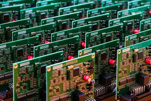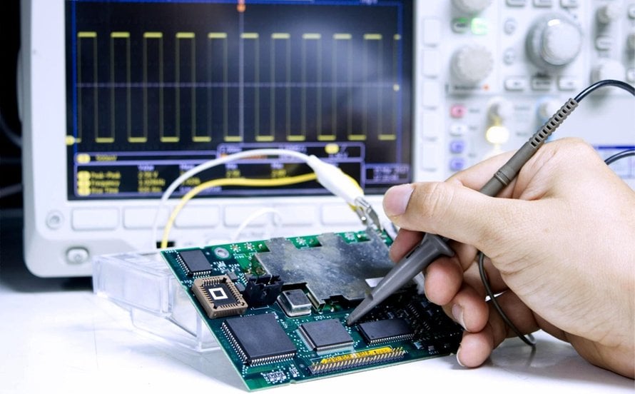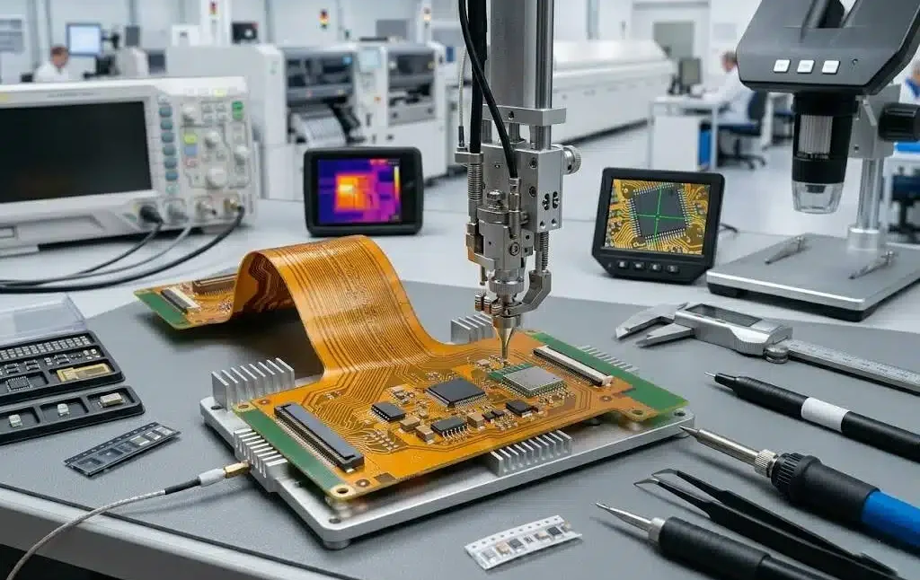
PCB Profiling: Routing, V-Score and Punching What Profiling Does Profiling is the step that separates the individual boards from the panel. It is one of the last operations in fabrication and one of the most consequential, because it sets the edge quality, the mechanical strength of the edge, the tolerance…
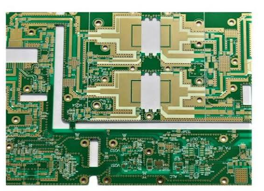
PCB Etching: Chemical Versus Laser Methods Two Ways to Remove Copper Etching is the step that turns a laminated copper sheet into conductors, and there are two practical ways to do it. Chemical etching dissolves unprotected copper in a bath, using a photoresist image as the mask. Laser etching removes…
PCB Copper Trace Current Capacity: How Much the Trace Can Carry Buyers and engineers often focus on the finished product and forget the production line behind it. In practice, most field failures can be traced back to process decisions made during assembly. Understanding PCB copper trace current capacity gives you…
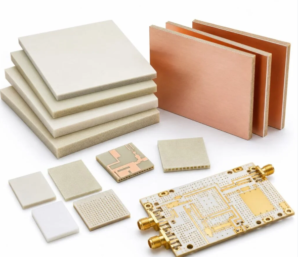
FR4 vs Rogers for RF Modules Why the Laminate Decides RF Performance At low frequency the copper does the work and the dielectric is a mechanical support. At radio frequency the dielectric becomes part of the circuit. Its permittivity sets the impedance of every trace and the physical length of…
SMT Reflow Solder Joint Void Reduction: Cutting the Gaps Inside Modern electronics depend on boards that are assembled correctly the first time. Every product – a phone, a charger, a medical instrument or an industrial controller – relies on thousands of solder joints that must conduct current for years. This…
PCB Laminate Resin Content: The Resin in the Board Electronics manufacturing has become a discipline of small details. Solder paste volumes, placement accuracy, temperature profiles and inspection limits all add up to the final result. This guide looks at PCB laminate resin content from the perspective of a PCBA factory…
Any-Layer HDI PCB: Design and Manufacture What Any-Layer Means In an ordinary multilayer board a via passes through the whole stack, and in an HDI board with a single build-up layer the microvias reach only the next layer. Any-layer HDI, sometimes called every-layer interconnection, goes further: a microvia can be…
SMT Stencil Tension: How Tight the Mesh Is Modern electronics depend on boards that are assembled correctly the first time. Every product – a phone, a charger, a medical instrument or an industrial controller – relies on thousands of solder joints that must conduct current for years. This article explains…
Solder Beading and Solder Ball Defects Two Different Defects Solder balls and solder beading are usually lumped together and should not be. A solder ball is a small sphere of alloy sitting on the surface, often on or beside a solder mask feature, and it is a contamination and short-circuit…
PCB Copper Trace Differential Impedance: The Pair Value Electronics manufacturing has become a discipline of small details. Solder paste volumes, placement accuracy, temperature profiles and inspection limits all add up to the final result. This guide looks at PCB copper trace differential impedance from the perspective of a PCBA factory…