ENIG PCB Cost: Gold Thickness, Layers and Volume
Electroless nickel immersion gold, known as ENIG, is the finish most engineers reach for when a board needs flat pads, long shelf life and a surface that survives multiple reflow cycles. It is also one of the more misunderstood items on a quotation, because the price depends on two thin layers whose thicknesses are measured in fractions of a micron and whose cost is driven by the gold market. This guide separates the parts of ENIG PCB cost that can be engineered and those that simply follow the process.
What ENIG Is and Why It Costs More
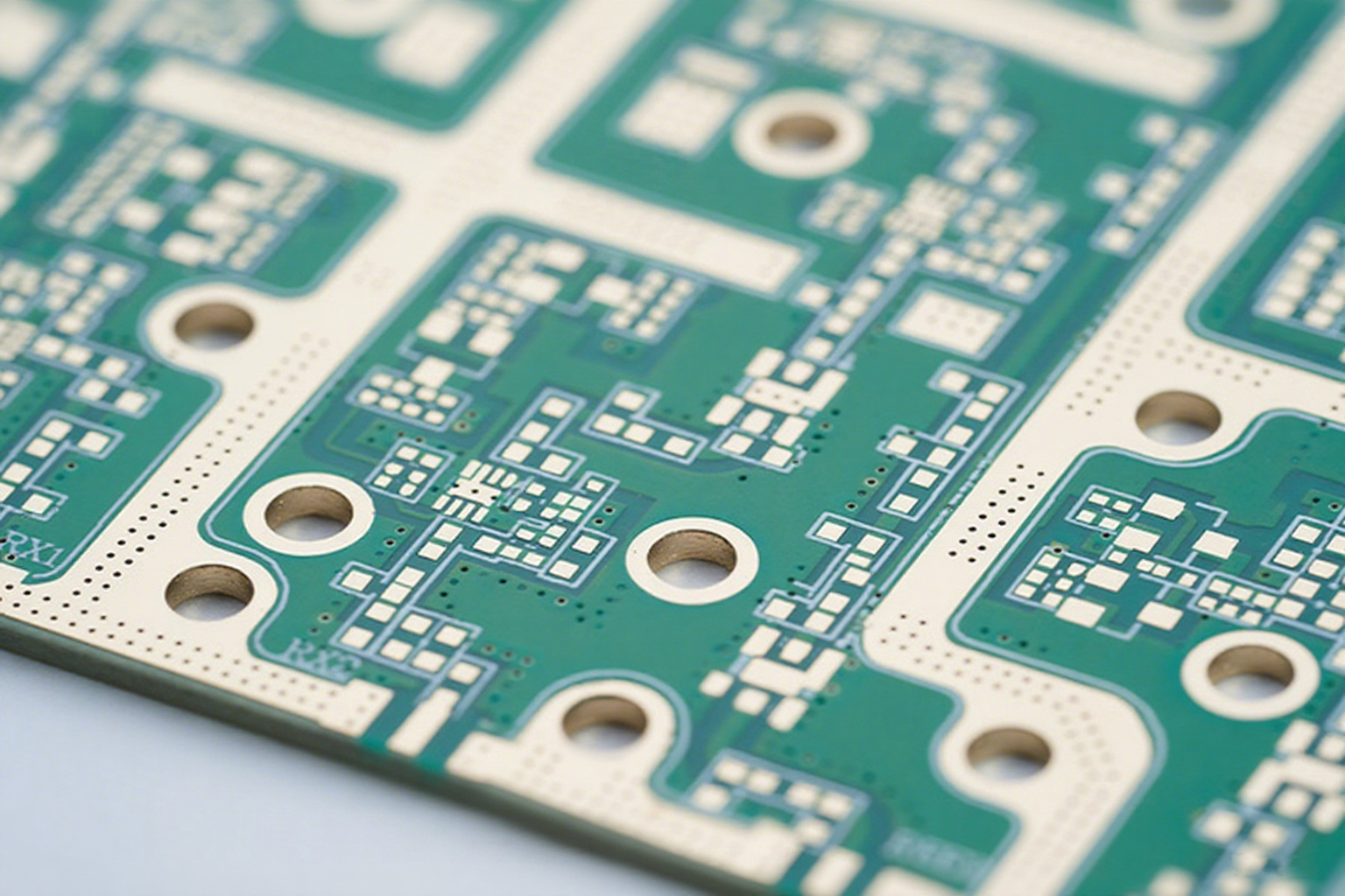
ENIG deposits a layer of nickel onto the copper by chemical reduction, then displaces a thin layer of gold onto the nickel by immersion. Because no electrical connection is needed, the process covers isolated pads and fine features uniformly. The nickel provides the wear and diffusion barrier, while the gold prevents the nickel from oxidising and keeps the surface solderable for a long period.
The cost comes from the process rather than the metal volume. Preparatory chemistry, bath control, temperature and time all have to be managed precisely, and the gold layer is thin enough that its contribution is meaningful but not dominant except on very large boards. What buyers pay for is a finish that is flat enough for fine pitch assembly and stable enough to store for a year. Where the design uses filled or plated over vias, the finish also has to be compatible with the via in pad or plated through structure chosen for the board.
Board Size and Layer Count
The size and complexity of the board set the baseline, and ENIG adds a roughly constant amount per unit area on top. As a reference point, five pieces of a standard two layer 100 by 100 mm board with ENIG finish typically quote between 45 and 80 dollars for the batch. The same quantity in a four layer board of 150 by 150 mm runs 90 to 150 dollars, and a six layer HDI board with ENIG reaches 180 to 350 dollars. Those figures assume a standard build time and normal panel utilisation.
In large volumes the picture changes. A standard two layer ENIG board ordered in quantities above five hundred pieces can reach 1.50 to 2.00 dollars per board, which is close to the price of the same board with a simpler finish. That convergence matters when a program is planning a long production run: the finish premium that looks significant at prototype quantity becomes almost irrelevant at volume.
Gold Thickness and Copper Weight
Gold thickness is specified rather than chosen freely. The usual standard is about 0.05 micron over a nickel layer of 3 to 6 microns, and increasing the gold to 0.1 micron adds roughly 0.10 to 0.20 dollars per square inch. Thicker gold is rarely needed for soldering; it becomes relevant for wire bonding or for connectors, and those applications usually move to a different finish entirely.
Copper weight affects the price indirectly. Moving from one ounce to two ounces adds about 0.50 to 1.20 dollars per board depending on size, because heavier copper needs longer etching and a more careful process. Fine features add cost as well: traces narrower than about 5 mil add 0.30 to 0.80 dollars per board, since they consume yield at both the imaging and the etching stage.
Where the Adders Come From
Via structures are the largest technical adder. Blind vias, buried vias and microvias increase the cost by 15 to 25 percent, because each adds a lamination cycle and additional drilling and plating operations. On an HDI board those steps are unavoidable, but on a board where they were added for convenience they are expensive convenience.
Lead time is the other large adder, and it is entirely optional. A standard build takes the normal production window, while an expedited order of forty eight hours typically adds 40 to 80 dollars per batch. Scheduling the prototype so that the expedited charge is not needed is one of the simplest cost reductions available on a development program.
Comparison With Other Finishes
Hot air solder levelling remains the cheapest option at roughly 0.08 to 0.12 dollars per square inch, but its surface is uneven and it is unfriendly to fine pitch parts. An organic solderability preservative costs about 0.05 to 0.08 dollars per square inch and performs well electrically, though its shelf life is short and it does not tolerate many reflow cycles. Immersion silver sits between them and offers good high frequency behaviour, but it tarnishes and requires controlled packaging.
ENIG is chosen when flatness and storage life matter more than the last few cents per square inch. On boards with ball grid arrays, land grid arrays or fine pitch connectors, the flatness advantage converts directly into assembly yield, and the extra cost is repaid by fewer defects rather than by better electrical performance. A newer variant, electroless palladium immersion gold, removes the nickel layer altogether and is used where black pad risk has to be eliminated, at a higher price.
<img src="https://www.gopcba.com/wp-content/uploads/2025/05/DIP拉线风彩.jpg" alt="Nickel and gold layer structure on an ENIG surface finish” />
Black Pad and Process Control
Black pad is the characteristic failure mode of the process. If the nickel surface is over-etched by the gold bath, the resulting joint is brittle and fails under thermal or mechanical stress even though it looked acceptable on inspection. The defect originates in bath chemistry and immersion time rather than in the design, which is why a fabricator that monitors its gold bath closely and records the results produces a more reliable board.
Control measures are well established. Nickel thickness is kept within a defined range, immersion time is limited, and the gold layer stays thin. Where a joint reliability problem appears across a batch, cross sectioning and analysis of the interface is the way to confirm it, and the broader principles of plating defect control are described in copper plating defects prevention.
Volume and Lead Time
Volume is the most powerful lever, but it takes time to reach. Prototype pricing at five pieces reflects engineering, tooling and set up rather than material, which is why a second order for the same design is noticeably cheaper. Once the design is stable and quantities rise, the ENIG premium per board falls to a small fraction of the total.
Process stability also improves yield, and the additives that maintain uniform deposition are part of that, as explained in electroplating additives for PCB. A partner such as gopcb records gold and nickel thickness data with each build, which means a change in the finish behaviour can be traced to a specific batch rather than discovered through a field failure.
FAQ
Is a thicker gold layer on ENIG better? Not for soldering. The standard 0.05 micron layer is sufficient, and thicker gold costs more without improving solderability. Wire bonding and connector applications use different finishes.
What causes black pad? Over-etching of the nickel surface by the immersion gold bath. It produces a brittle joint that fails under stress, and it is prevented by controlling bath chemistry, nickel thickness and immersion time.
How much cheaper is HASL than ENIG? Roughly 0.08 to 0.12 dollars per square inch for HASL against a higher ENIG figure, but HASL is unsuitable for fine pitch assembly and does not provide the same shelf life.