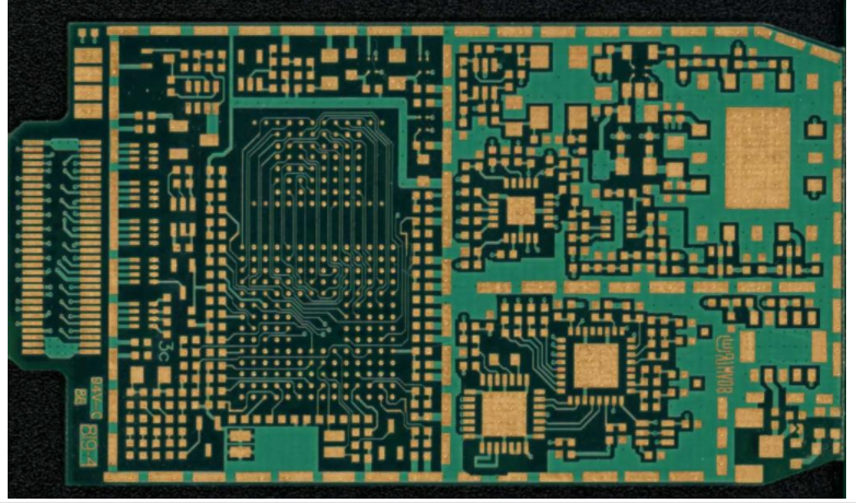
Board Warpage, Bow And Twist Control
A printed circuit board is supposed to be flat, and in practice it never quite is. The laminate expands and contracts as it is pressed, drilled and soldered, the copper on each layer has a different expansion behaviour from the resin that surrounds it, and the result is a board that bows like a shallow dish or twists about its diagonal. Some of that is unavoidable, and the question is how much is acceptable and how much can be designed out.
This article distinguishes the terms, explains where the movement comes from, how it is specified and measured, why it matters to assembly, and what can be done about it.
What Bow And Twist Mean
Bow is a curvature across the board in one direction, like a dish or a dome, and it is measured as the maximum deviation from a flat plane divided by the length of the board. Twist is a distortion about a diagonal, so that two opposite corners lift while the other two drop. Warpage is the general term that covers both, and it is normally what a customer means when the board does not sit flat.
The conventional way to measure is to place the board on a flat surface and measure the gap under it with a gauge, then to hold the board down at three corners and measure how far the fourth corner lifts. The second measurement is the one that reveals twist, and the two are usually reported together as a percentage of the diagonal. Both are covered by the same acceptance limit, so the term bow and twist is normally written as one requirement on the drawing.
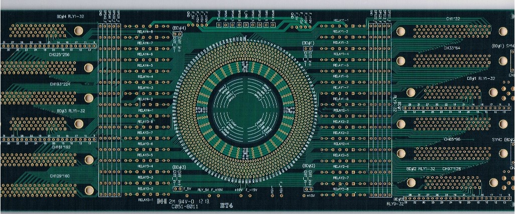
Where The Movement Comes From
The main cause is asymmetry. A stackup with more copper on one side of the centre than the other will bend towards the copper when it cools, because the copper and the resin contract by different amounts. Odd layer counts, asymmetric prepreg thicknesses in the same stackup, and heavy copper on one outer layer only all produce the same result, and the effect can be predicted well enough during design to be designed out.
Even a balanced stackup moves, because the pattern of the copper is not symmetric even when its weight is. A plane on one layer and a grid of traces on the corresponding layer on the other side will behave differently during pressing and during reflow, and the board may be flat after fabrication and bend only after it has been through the soldering oven. That second stage is where most complaints originate.
Press, Drill And Reflow
The press cycle sets the residual stress in the laminate. The resin has to flow and cure at temperature, and the way the panel is cooled and how long it is held under pressure decide how much stress remains locked in the board. A press profile that is short or hot leaves more stress, and the stress is released later, when the board is heated again for assembly.
Drilling removes material and redistributes the internal stress, so a panel can change shape after drilling, and a board with many large holes is more likely to move than one with few small ones. Reflow then heats the whole assembly above the glass transition of the resin, at which the material is soft enough to relax and the copper is free to dominate. All three stages add to the same total, and the flatness that is delivered is the sum of them.
Why It Matters
The first consequence is assembly. A warped board does not sit flat on the printer nest, so the stencil gap varies and the paste deposit varies with it, which produces joints that differ across the panel. A warped board also feeds badly into a placement machine and can jam a conveyor or a magazine, and it can lift off the support pins in a reflow oven and sag further.
The second consequence is mechanical. A board that is clamped flat during assembly holds the stress until the fixings are released, after which it pulls on the solder joints. That load is applied to the smallest joints on the board, and it is a recognised cause of cracked chip capacitor terminations and of open joints on fine pitch packages. Related joint behaviour is described under SMT component shift causes.
Specification And Measurement
Flatness is specified as a maximum percentage of the diagonal, commonly 0.75 percent for a surface mount board and 1.5 percent where the assembly process can tolerate more. The figure applies after reflow as well as before it, and a specification that mentions only the delivered condition will not cover the case that actually causes problems. The measurement method, the support conditions and the temperature at which the board is measured should all be stated alongside the figure.
Two conditions are sometimes added. One restricts the movement over the area where fine pitch components are placed, because a local bump under a ball grid array causes more trouble than a gentle bow across the whole panel. The other restricts the material and the stackup, since the flatness that can be achieved depends on both. The dimensional behaviour of the laminate itself is discussed under PCB dimensional stability and expansion.
What Can Be Done About It
Design has the largest influence and provides the cheapest remedies. Balancing the copper weight on either side of the centre, using a symmetrical construction, and avoiding a stackup where one outer layer carries a plane and the other carries only traces will remove most of the risk. Where a heavy plane is required on one side, a mesh rather than a solid pour on the other side is sometimes used to match the behaviour, and the choice is discussed under copper flooding, mesh or solid.
Process has the rest. A longer press cycle with a controlled cooling ramp reduces the residual stress, a bake before assembly relieves some of it, and supporting the board properly through the oven prevents the sag that becomes permanent when the resin softens. The stackup decisions behind all of this are described under balanced stackup and odd layer count and under layer stackup from one to eight layers.
Panelisation, Thickness And Hole Density
Flatness is easier to hold on a thin board than on a thick one, and easier on a small one than on a large one, which is why a specification that quotes a single percentage for every product is unrealistic. Thin laminate flexes under its own weight and needs support but returns to flat, while thick laminate holds the stress and bows permanently. A thick panel with a high copper content and a large drilled area is the worst combination, because it has the most internal stress and the least ability to relieve it.
Panelisation adds a further constraint. A panel that is scored rather than routed has a web of material between the boards that resists movement, while a routed panel is a frame of thin material that moves freely. The frame is often what warps, and it can carry the boards with it, so a panel that is difficult to hold flat may be improved by changing the break method rather than by changing the laminate.
FAQ
Does baking reduce warpage? It can, because heating the board above the glass transition allows some of the locked in stress to relax, and it is often done before assembly for that reason. The effect is partial and it cannot correct a fundamentally unbalanced stackup.
Is a warped board always rejected? No. Whether it is acceptable depends on the assembly process and on the components, and the decision should be made against the specification rather than by appearance.
Can a board be flattened after it is built? It can be pressed hot between flat plates, and this is sometimes done for a small panel, but the treatment is a stress relief rather than a cure, and the board will move again when it is reheated for assembly.