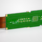
Optical Imaging PCB: Design for Cameras, LiDAR and Fiber Modules
An optical imaging PCB sits between a sensor and a processor, and the requirements on it come from physics rather than from a feature list. Photons arrive at a sensor, electrons leave it at high speed, and in a LiDAR or fiber module a laser must be driven and cooled in the same small volume.
The three product families, cameras, LiDAR and optical transceivers, share the same design problem in different proportions: a dense fine-pitch interconnect, a high-speed data path, and a thermal path that must remove heat from a device that cannot tolerate much temperature change.
What the Board Has to Do
The board carries the sensor, performs the impedance-controlled transition from the sensor output to a processor or a serializer, delivers clean power to an analog front end, and provides a mechanical reference that keeps the optical axis aligned.
Mechanical reference is the function designers underestimate. In a camera module, a fraction of a degree of tilt translates into image degradation, and the board flatness and mounting features are part of the optical design rather than a mechanical afterthought.
Sensor Interconnect and Fine Pitch
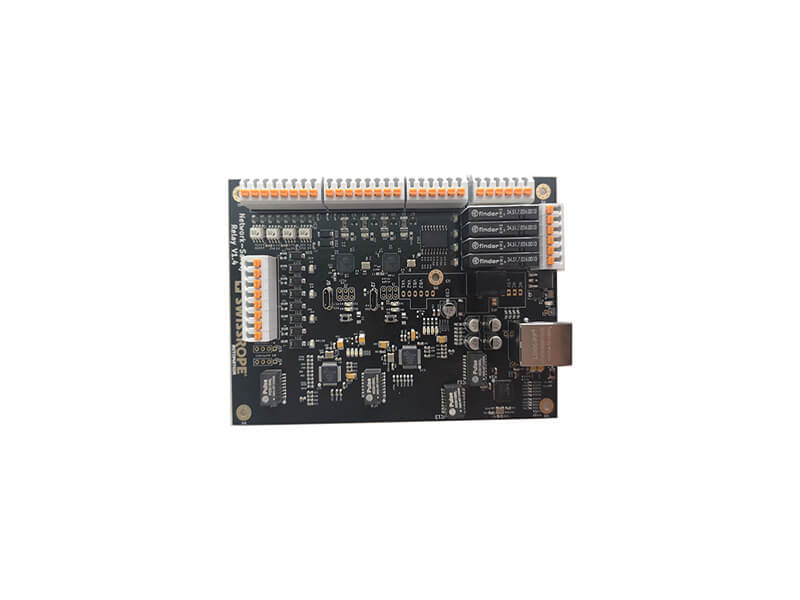
Image sensors and optical engines present hundreds of connections at a pitch that demands fine lines, small vias and sometimes via-in-pad. The escape routing determines the layer count, and the layer count determines the cost.
Bonding temperature is a constraint in modules where the sensor is attached after assembly. A board that has already been through reflow will see additional heat, and the materials and finishes must tolerate that second excursion without change in flatness or cleanliness.
Cleanliness matters more here than on a general-purpose board. Particulate contamination on a sensor surface becomes a permanent defect in every image, so assembly and handling procedures are part of the board specification.
High-Speed Signal Integrity
Sensor data rates have risen to the point where the interface behaves as a transmission line. MIPI and similar links are differential, impedance controlled and length matched, and their routing budget is measured in a few tens of millimetres.
That constraint changes the architecture: the processor is placed next to the sensor, and the long connection is made at a higher speed by a serializer, which moves the problem to a different interface rather than eliminating it.
Reference plane continuity is the single most important layout rule. A split under a differential pair forces the return current to detour, and the result is radiated emissions and a degraded eye diagram that no amount of equalisation fully recovers.
Low-Loss Materials and Layer Choice
At the data rates used in modern imaging systems, standard FR-4 loss becomes significant over even a short trace. Where the interface is fast and the routing is not short, a low-loss material is used for the signal layers that carry it.
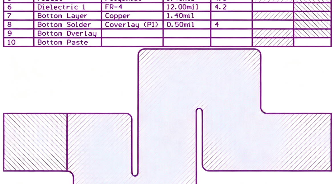
Hybrid stackups are common: low-loss laminate for the high-speed layers and standard FR-4 elsewhere. That keeps material cost proportionate, since the mechanical and power layers do not benefit from a low-loss dielectric.
Where a low-loss material is used, the impedance geometry changes because the dielectric constant is different. A design copied from an FR-4 stackup will not produce the intended impedance, so the stackup and the geometry must be calculated together.
Thermal Management
Thermal management has two distinct targets on an imaging board. The sensor must be held near a stable temperature for noise performance and, in some devices, to avoid dark current drift; the laser or the processor must be cooled to remain within its rating.
Those two requirements sometimes conflict, because the heat source and the sensitive device are close together. The usual solution is to separate them thermally: keep the laser on a copper island connected to the enclosure through thermal vias, and keep the sensor on a separate island with its own reference.
Thermal vias, copper pours and a mounting design that couples heat into the frame are the tools. Where the module is sealed, conduction is the only path, and the board becomes part of the thermal structure.
Noise and Analog Front Ends
Imaging front ends include sensitive analog circuitry: the analog supply for the sensor, reference generation and sometimes a transimpedance stage in a fiber receiver. Those circuits require a quiet supply and a clean ground reference.
The switching regulator that powers the module is the main noise source, and its placement and its loop area determine how much of that noise reaches the analog domain. Keeping the switching loop small, placing the regulator away from the sensor, and providing local decoupling at every analog pin are the standard measures.
Ground partitioning matters as much. The analog measurement ground and the digital ground should meet at one defined point, usually beneath the converter or the processor, so that the return currents do not share a conductor.
Mechanical and Optical Alignment
The board holds the sensor in a defined position relative to the lens, the laser and the fiber. Tolerances on mounting holes, board thickness and flatness therefore propagate directly into optical alignment.
Board thickness tolerance matters where the sensor sits on one side and a lens mount references the other. Thickness variation moves the focal plane, and the optical design must accommodate the full tolerance band or the board must be specified more tightly.
Flatness is equally important. A board that bows after assembly tilts the sensor, and the tilt may not be correctable by focus adjustment because it is not a simple translation.
Assembly and Handling
Imaging modules use fine-pitch assembly and often a second operation to attach the optical component. Board handling therefore includes cleanliness control, anti-static protection and often a carrier that keeps the board flat through both operations.
Test access must be designed in, because probing a fine-pitch pad after the optical part is attached is impractical. Test points on the panel or a dedicated test connector that shares pins with the interface are the usual answers.
Cost Structure
Cost is driven by the layer count needed for the escape, the fine-line capability, the material choice, and the cleanliness and inspection requirements. Yield is a factor, because a defect that would be cosmetic on a general-purpose board is fatal in an imaging module.
Where the design can reduce the layer count by changing the escape strategy, or restrict the low-loss material to the layers that need it, the saving is direct. Both changes are layout decisions rather than material substitutions.
Design Checklist
Confirm the interface length and loss budget, verify plane continuity under every high-speed pair, check the thermal path from the laser and the processor into the enclosure, and confirm the board flatness and thickness tolerance against the optical requirement.
Then review the analog supply and the ground arrangement. On an imaging board, the noise performance of the front end usually determines the image quality more than any digital design choice.
Related reading: FPGA board high-speed interfaces, high-frequency data bus routing, and via in pad versus plated through.
FAQ
Why does my camera image show fixed pattern noise? Fixed pattern noise usually originates in the analog supply or the ground reference rather than in the sensor. Check the decoupling at the sensor pins and the return path under the analog supply.
Is via-in-pad required for sensor escape? Only when the pitch leaves no alternative. Where a staggered via can be used, the process is simpler and the assembly risk lower.
Does the board thickness really affect focus? Yes, because the sensor and the lens mount reference opposite faces. Thickness variation moves the focal plane, so the optical design must allow for the full tolerance band.