Backdrilling And Stub Removal In High Speed Boards
A plated through hole that only needs to connect the outer layers still passes through the whole board, and the unused portion below the last connected layer is called a stub. At high frequencies the stub behaves as a resonant transmission line and degrades the signal that passes through the via.
Backdrilling removes the stub by drilling the hole again from the opposite side to a controlled depth. It is a mechanical process with tight tolerances, and it is one of the few ways to recover signal integrity after the stackup has already been fixed.
Why Stubs Matter
A stub is an open circuited transmission line attached to the signal path. It reflects energy at frequencies related to its length, and the resulting dips in insertion loss become deeper and appear at lower frequency as the data rate rises. On a long stub the effect can be seen well below 10 GHz.
The problem is worst for a via that connects only the outer layers of a thick backplane, because that via has the longest possible stub. A connector via in a 4 mm board can have a stub of nearly 4 mm, which is a serious discontinuity at 25 gigabits per second. The via structures involved are described under via in pad or plated through.
What Backdrilling Does
Backdrilling removes the unused barrel by drilling from the side opposite to the last connected layer, using a bit slightly larger than the original hole. The bit cuts away the plating and the resin down to a controlled depth, leaving the remaining barrel intact and connected.
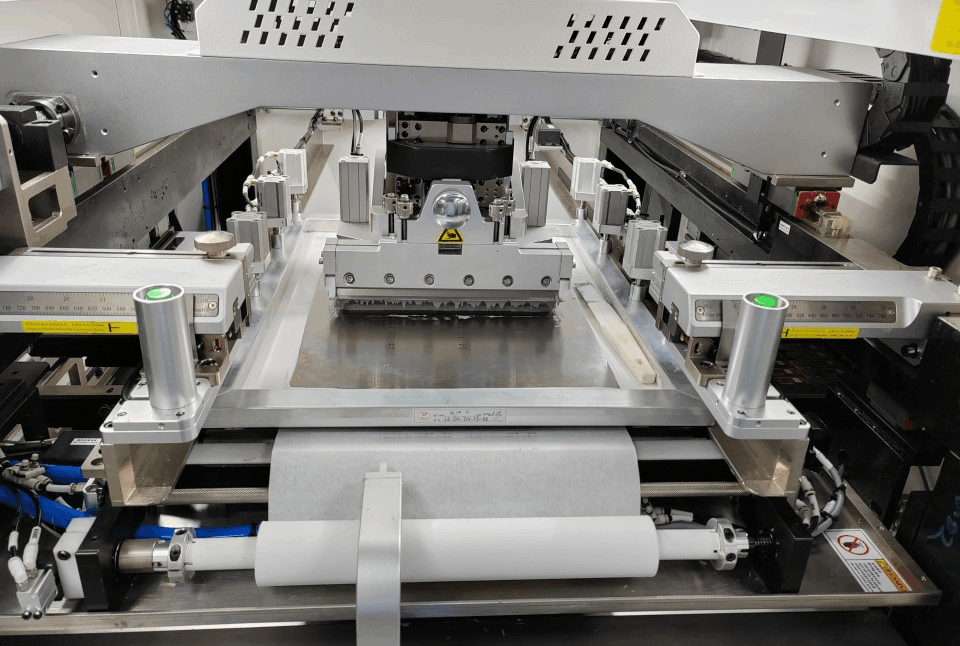
The process is done after plating and before the surface finish, and it is normally performed on a dedicated machine with depth control better than plus or minus 0.1 mm. The resulting hole is slightly larger at the backdrilled end, which has to be accounted for in the keepout around the via.
Drill Depth And Tolerance
Drill depth is measured from the surface to the point where the bit stops, and the target is a small remaining stub rather than none at all. Leaving a short stub is safer than cutting into the layer below, because the plating of that layer would be damaged.
A typical remaining stub is 0.2 to 0.4 mm, and the tolerance on the depth has to be tighter than the distance to the next layer. Where the layers are close together, the process capability of the machine sets the minimum safe stub.
Effect On Signal Integrity
Removing the stub raises the frequency at which the first resonance appears, which moves the dip above the band of interest. The improvement in insertion loss at the top of the band can be several decibels, and the return loss improves as well.
The benefit is largest for thick boards and for vias that connect few layers, and smallest for a short via in a thin board. Whether backdrilling is worth the cost is a calculation based on data rate and stack height rather than a general rule. The stackup decisions behind it are described under layer stackup from one to eight layers.
Manufacturing Considerations
Backdrilling adds a process step, an extra alignment and a risk of damaging the hole. The bit must be aligned to the original hole within a small fraction of its diameter, and the panel must be held flat so that the depth is consistent across the whole board.
The larger hole also affects the copper keepout and the solder mask opening, and it can reduce the annular ring available on the backdrilled side. Those points have to be agreed with the fabricator before the stackup is released.
Verification And Inspection
Depth is verified on a sample by cross section, which shows the remaining stub and the condition of the barrel. A time domain measurement on a test coupon gives the electrical result, and the two are used together to confirm both the geometry and the performance.
Samples should be taken from the first panel of a job and after any change of bit or setup, because depth depends on the machine and on the material. How the requirement is written for the fabricator is described under PCB design and fabrication.
Process Control and Verification
On a design of this kind, stub is the item that decides how the rest of the board is arranged. The process window is set by the narrowest step in the flow, so an improvement anywhere else shows up as margin rather than as yield until that step is addressed. A short note on the drawing about handling, storage or packaging is often worth more than an extra decimal place on a tolerance.
Where a value sits close to a process limit, the drawing should say so, since the shop can then open the process window rather than working to a nominal figure that carries no tolerance. A stack-up that is drawn rather than described removes most of the ambiguity from a quotation, and it lets the fabricator price the board against the dielectric and copper weights that will actually be used.
Where the requirement is not written down, the shop supplies its own default, and the default is chosen for the process rather than for the design. The measurements that matter are the repeatable ones: conductor width and spacing, annular ring, finished hole size, plating thickness and surface finish are all verifiable on a coupon that travels with the panel.
Process Control and Verification
On a design of this kind, stub is the item that decides how the rest of the board is arranged. The process window is set by the narrowest step in the flow, so an improvement anywhere else shows up as margin rather than as yield until that step is addressed. A short note on the drawing about handling, storage or packaging is often worth more than an extra decimal place on a tolerance.
Where a value sits close to a process limit, the drawing should say so, since the shop can then open the process window rather than working to a nominal figure that carries no tolerance.
Process Control and Verification
On a design of this kind, stub is the item that decides how the rest of the board is arranged. The process window is set by the narrowest step in the flow, so an improvement anywhere else shows up as margin rather than as yield until that step is addressed. A short note on the drawing about handling, storage or packaging is often worth more than an extra decimal place on a tolerance.
A first article check confirms that the process and the drawing agree on the points listed above, and that the coupon data supports the values used in the design.

Where a measurement falls outside the expected window, the sample is retained so that the cause can be established before the balance of the batch is released.
FAQ
Does every high speed board need backdrilling? No. It is worth considering when the stub is long relative to the wavelength at the highest frequency of interest, which usually means thick boards and data rates above about 10 gigabits per second.
Can backdrilling be done after assembly? No. It is a fabrication step performed before the surface finish, and it cannot be added to a finished board without destroying it.
How much stub should remain? A short remaining stub of 0.2 to 0.4 mm is the usual target. Removing all of it risks cutting into the next layer, which is a far more expensive failure than a small stub.