PCB Prototype Flow: From Design Files to Shipped Samples
A prototype order is not simply a small production run. It is a manufacturing task with different economics, different risks and a much tighter feedback loop, because the purpose of the build is to answer questions rather than to ship volume. Understanding each step of the PCB prototype flow helps a design team predict where time is actually spent and which details cause a delay.
What a Prototype Build Actually Involves
A prototype moves through the same sequence as production: data preparation, material release, inner layer imaging, lamination, drilling, plating, outer layer imaging, mask and finish, electrical test and final inspection. What differs is that every step runs with almost no margin for rework, since the panel quantity is too small to absorb scrap.
That is why a prototype shop pays disproportionate attention to front-end engineering. Catching an ambiguity in the data package costs an hour; catching the same problem after lamination costs the whole build.
Design File Review Before Anything Is Ordered
The design file review is the first gate. The shop checks that the Gerber or ODB++ set matches the layer count, that the drill file references the right apertures, that the outline closes, and that the soldermask and paste layers agree with the copper. A surprising share of delays trace back to a revision mismatch between files that were released at different times.
A complete package also includes the stackup drawing, impedance requirements, surface finish, board thickness and tolerance, and any controlled impedance coupon definition. Supplying all of it once is faster than answering questions over three days.
DFM Feedback and Panelization
Design for manufacturability feedback follows the file review. The fabricator flags features that fall below the process minimum: annular rings that are too small, traces that crowd a via, mask dams narrower than the screen can hold, or a component keep-out that overlaps the panel border. Most of these are fixable in the layout without changing the circuit.
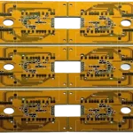
Panelization decides how many boards fit on a production panel and whether the prototype can share that panel with other work. Adding breakaway rails, tooling holes and fiducials at this stage is what allows the same design to move smoothly into assembly later.
Material and Stackup Selection
Prototype material choice sets the baseline for everything that follows. FR-4 covers most digital designs, while a high Tg grade is worth the premium when the board will see lead-free reflow or wide thermal cycling. High-speed designs may need a laminate with a specified dielectric constant and loss tangent so that impedance calculations hold after fabrication.
Deciding the stackup at prototype stage avoids a painful redesign later. If the product is likely to grow from four layers to six, define the layer functions now so that the added layers are planes and not signal layers that force a complete re-route.
Imaging, Etching and Layer Registration
Inner layers are imaged, developed and etched, then inspected before lamination. Registration between layers is the critical parameter: a stack that is bolted together correctly but exposed slightly off-center produces an intermittent via connection that passes continuity test and fails in the field.
Direct imaging has made this far more repeatable than film-based exposure, because the same digital data drives every layer. On a prototype, where the panel count is too small to justify tooling, that repeatability is exactly what makes a one-off build predictable.
<img src="https://www.gopcba.com/wp-content/uploads/2020/12/project_image_2.jpg" alt="First article inspection of a prototype PCB with coupons on the panel” />
Drilling, Plating and Via Reliability
Drilling sets the smallest via the design can use, and plating determines whether that via survives thermal stress. Aspect ratio is the number to watch: the ratio of board thickness to finished hole diameter. Beyond roughly 8:1, plating uniformity inside the barrel becomes difficult to guarantee without special process control.
For high-reliability programs, a thermal stress test or microsection on a coupon from the same panel is the only direct evidence that the plating is sound. Prototype quantities make that coupon easy to include, and skipping it is a false economy.
Solder Mask, Surface Finish and Silkscreen
Surface finish is chosen for the assembly process, not for appearance. Hot air solder leveling remains cost effective for through-hole work, while electroless nickel immersion gold and immersion silver suit fine-pitch SMT and long shelf life. The right answer depends on how the board will be stored and how many reflow passes it will see.
Silkscreen placement is a small detail with real consequences. Reference designators that overlap a pad, or a pin-1 marker hidden under a component, slow down assembly and invite a placement error. Reviewing silkscreen against the assembly drawing takes minutes and prevents a scrapped batch.
Electrical Test and First Article Inspection
Electrical test confirms continuity and isolation against the netlist. On a prototype it is common to test the whole panel rather than the individual boards, which is why a netlist file must accompany the Gerber data. Without it, the shop can only perform visual inspection.
First article inspection goes further and checks dimensions, hole sizes, finish thickness and impedance coupons against the drawing. When the first article matches, the design is released for a larger sample build with confidence rather than hope.
Packing and Prototype Turnaround
Fast prototype turnaround comes from compressing queue time rather than machine time. A shop that runs a dedicated prototype line, keeps common laminates on the shelf and quotes working days honestly will beat one that promises the impossible and then negotiates.
The most effective way to shorten a build is to send a clean data package on the first attempt. A design team that runs its own design and fabrication review before release avoids the round trips that consume most of a week, and reviewing multilayer prototype requirements early prevents stackup surprises.
Documentation That Ships With the Prototype
A prototype is far more useful when it arrives with data. Ask for the fabrication drawing returned with as-built values, the impedance report if the stackup was controlled, and a copy of the panel layout showing where each board sat. Those records make it possible to correlate a failure with a specific panel position instead of guessing.
It also helps to keep a serialized traveler for every build. When the second prototype behaves differently from the first, the material lot, the plating line and the cure profile are the first variables to compare, and none of them can be reconstructed reliably after the fact.
Record those process notes alongside the manufacturable PCB design guidelines used during the review, so the next revision starts from a known baseline rather than an assumption.
FAQ
How long should a prototype take? A straightforward two to four layer board with a complete data package typically runs in two to five working days. Adding impedance control, a non-standard laminate or a tight tolerance extends the schedule because those steps introduce additional queue and test time.
Is it cheaper to order ten boards than five? Often yes. Setup and tooling dominate the cost of a small order, so the incremental material and machine time for a few extra pieces is small. Ordering enough boards to cover assembly and debug usually costs less than placing a second order later.
What causes most prototype delays? Incomplete or inconsistent data. A missing netlist, a stackup that does not match the drawing, or a drill file that disagrees with the pad sizes will stop a build faster than any process issue, and see PCBA development process planning for the follow-on assembly steps.