PCB Short Circuit Causes in Fabrication and How to Prevent Them A short circuit that passes a low-voltage electrical test and fails after assembly is one of the more frustrating defects a board can carry, and also one of the better documented, because the mechanism is understood. In most cases…
PCB Electrical Test Methods: Flying Probe and Grid A finished board that leaves the shop with an undetected open circuit does not simply get scrapped. It travels to the assembly line, collects components, passes through reflow and possibly through in-circuit test, and only then reveals the defect, at which point…
Lamination Voids and Delamination: Causes and Process Control Delamination and lamination voids are the failure modes that pass every electrical test on the day of manufacture and reappear months later as a blister or a lifted pad. They form when the resin in the prepreg does not completely fill the…
Six-Layer Stackup Options: Signal, Ground and Power Layers A six-layer board is the first stack that gives a designer a dedicated ground plane and a dedicated power plane without giving up two routing layers. That is why it has become the default for consumer products, industrial controllers and anything with…
Timing Analysis in High-Speed PCB Design Timing analysis is the part of high-speed design that decides whether a bus will actually work, and it is the part most often skipped because it happens before any routing exists. Once an interface runs at hundreds of megabits and the edge rates fall…
8-Layer PCB Prototype Fabrication: Lamination to Copper An eight-layer board is not simply a six-layer stack with two more cores. Once the layer count rises, the fabrication route gains a full lamination cycle, the inner cores must be treated before they are bonded, and the plated barrels become long enough…
Common Impedance Coupling: Grounding Techniques That Suppress It Ground is supposed to be the quiet reference that every signal is measured against. In practice it is a conductor with resistance and inductance, and when two circuits share a portion of it, the current from one appears as a voltage in…
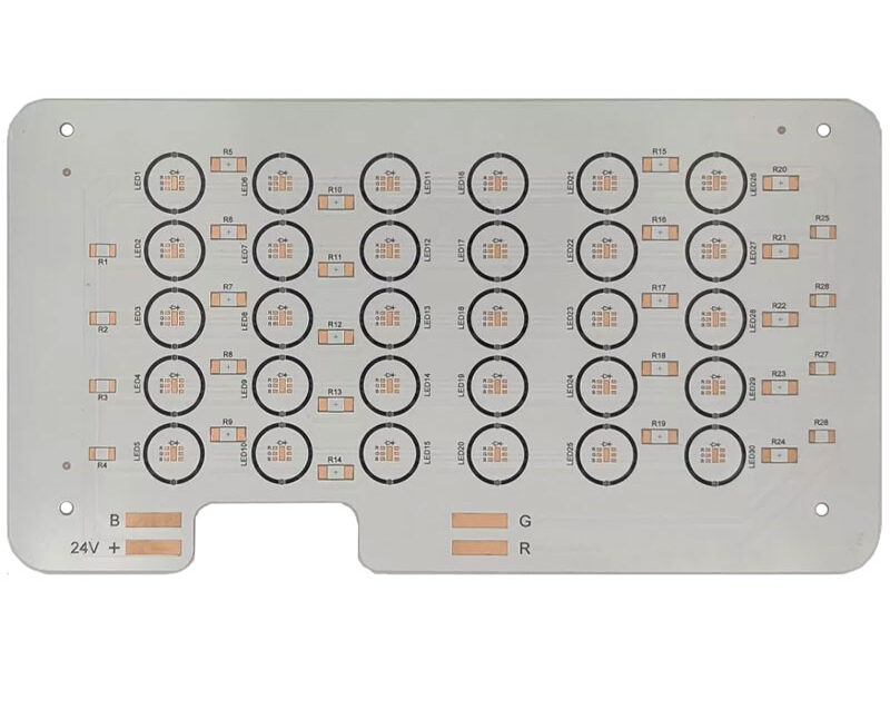
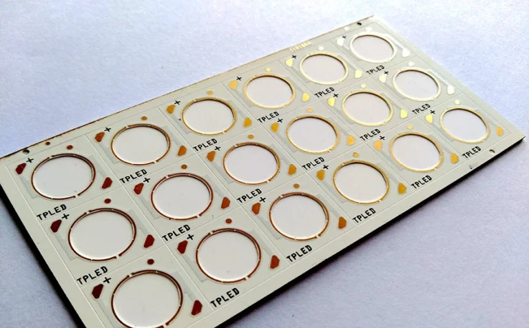
Single-Sided PCB Design and Double-Sided Boards: Structures and Uses Not every product needs eight layers. A large share of electronics, from power supplies and relays to LED drivers and simple instruments, is built on one or two copper layers, and those boards are successful because the design was matched to…
PCB Layout Review: Four Checks Before You Release the Board The review that happens after the routing is finished is the last chance to catch problems before tooling is committed. At that stage the electrical intent is fixed, so the questions shift to whether the board can be built, whether…
PCB Design Workflow: Ten Steps From Schematic to Release Files Board design fails more often from missing inputs than from bad routing. A layout engineer who receives an incomplete schematic, an approximate mechanical drawing, and a verbal description of the stackup will produce a board that matches none of them…