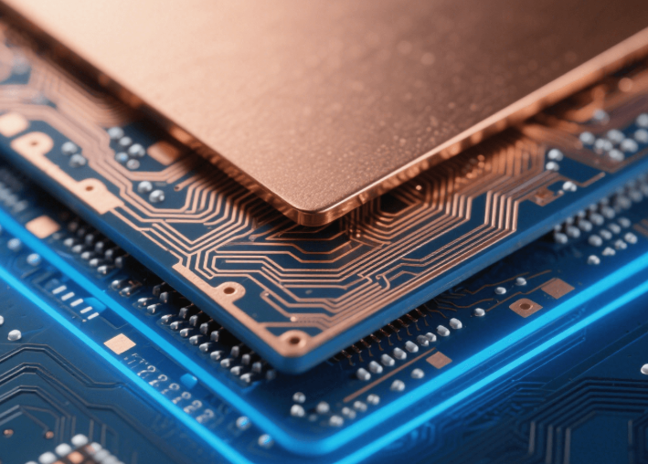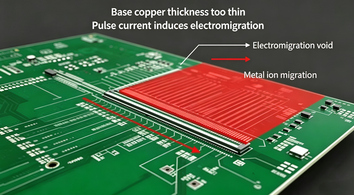
As high-speed memory and processor interfaces continue to increase in bandwidth, PCB designers must pay closer attention to more than routing, impedance, and layer stackup. PCB copper thickness at critical component interfaces can also affect long-term reliability, particularly when BGA packages carry high-density transient or pulse currents. In applications such…
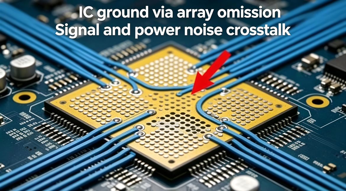
In high-speed PCB design, the ground via array beneath a BGA package is easy to overlook. Engineers may confirm that a continuous ground plane exists and assume that the return-current path is therefore sufficiently low impedance. At high frequencies, however, a continuous ground plane alone does not guarantee an effective…
When choosing a PCB assembly method, manufacturers typically consider two major technologies: Through-Hole Technology (THT) and Surface Mount Technology (SMT). Both technologies have unique advantages and are suitable for different electronic products and manufacturing requirements. The choice between THT vs SMT can significantly affect PCB assembly cost, component density, production…
When a high-speed PCB design is migrated from one EDA platform to another, engineers often focus on whether the schematic, layer stackup, routing geometry, and component information have been transferred correctly. However, an equally important issue can be hidden in the design metadata: differential pair definitions and other electrical constraints…
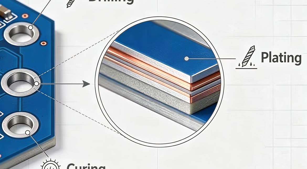
In high-volume PCB production, unnecessarily customized via dimensions can become an overlooked source of manufacturing complexity. Engineers sometimes select different hole diameters and pad sizes to accommodate local routing requirements without considering the downstream impact on drilling, plating, inspection, and production scheduling. Although a small dimensional change may appear insignificant…
As electronic products continue to become smaller, smarter, and more powerful, PCB assembly technology has evolved to meet increasingly demanding requirements for miniaturization, reliability, production efficiency, and electrical performance. Today, two major component mounting methods are widely used in electronics manufacturing: Surface Mount Technology (SMT) and Through-Hole Technology (THT). Although…
During the PCB design stage, engineers sometimes assume that customized colors automatically make a product look more premium. Choosing black, white, or other customized solder mask colors, however, may introduce additional material costs, process requirements, inspection challenges, and production lead time. For most industrial control, power electronics, general consumer electronics,…
Bioelectric signals such as electrocardiography (ECG) and other physiological signals are typically low-level analog signals that can be highly sensitive to electrical interference. Their acquisition circuits often have high input impedance, making them particularly vulnerable to leakage current, parasitic capacitance, electromagnetic coupling, ground noise, and environmental changes. For this reason,…
In multilayer PCB manufacturing, prepreg is an essential material used to bond copper layers and form the dielectric structure of the finished board. When optimizing a PCB Stackup, many projects face a difficult balance between electrical performance, material cost, manufacturing yield, and long-term reliability. Two common approaches can create unnecessary…
PCB Prototype production is typically carried out in small quantities to verify circuit performance, mechanical fit, and manufacturing feasibility. At this stage, manufacturers can often accommodate designs that are not fully optimized for automated, high-volume production. However, a design that works well for prototypes may encounter significant problems when transferred…