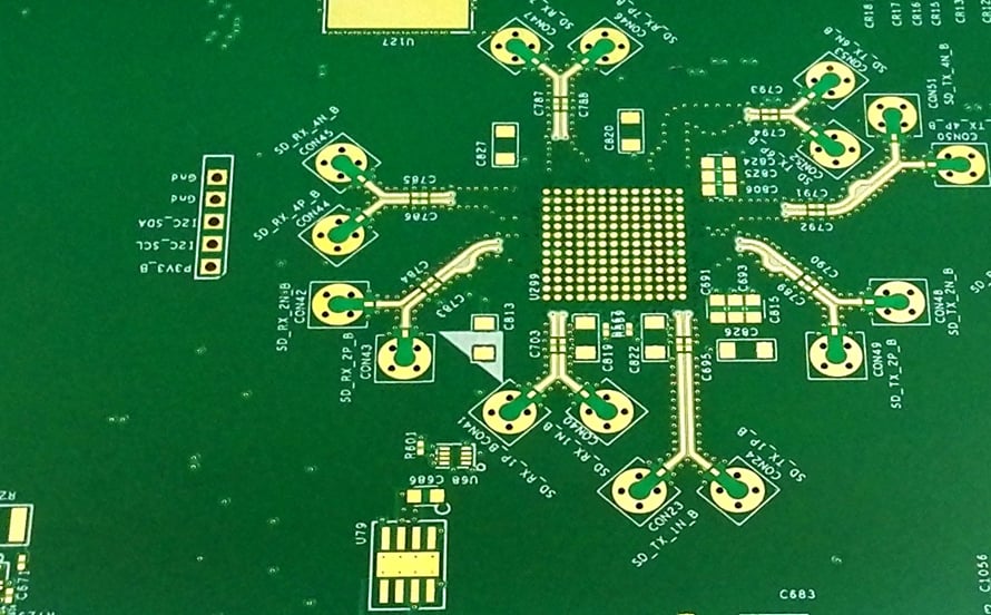
Many recurring PCB production redesigns are not caused by manufacturing equipment failures or process problems. In many cases, the underlying issue can be traced back to insufficient PCB DFM review during the prototype stage. Engineers often focus on whether a prototype functions correctly, whether the board powers on successfully, and…
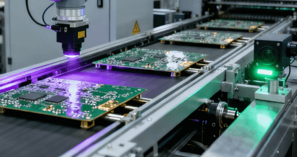
In PCB manufacturing, prototype development is often accompanied by multiple rounds of design optimization. Engineers may adjust component placement, routing, layer stackup, impedance parameters, hole dimensions, materials, or manufacturing processes after each prototype build. These changes are normal during product development. The real risk occurs when updated design files, manufacturing…
In high-speed multilayer PCB design, engineers often rely on the dielectric constant (Dk) provided in a laminate datasheet when calculating controlled impedance. The problem is that a Dk value measured at a low frequency cannot always accurately represent the electrical behavior of the same material at hundreds of megahertz or…
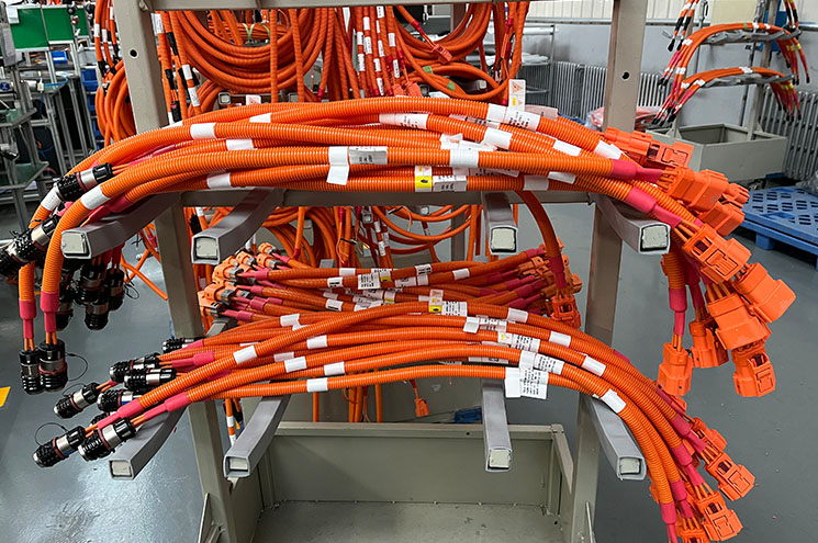
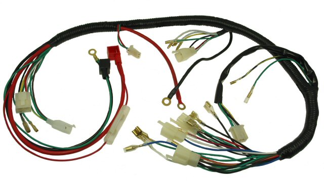
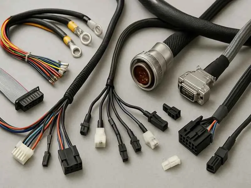
A wire harness is an engineered electrical assembly that organizes multiple wires, terminals, connectors, and protective components into a defined routing structure. By integrating individual conductors into a pre-assembled unit, a wire harness simplifies installation, improves wiring consistency, and supports reliable power and signal transmission inside electronic and electrical equipment.…
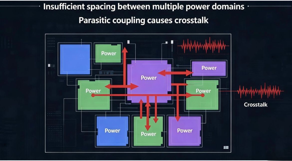
In mixed-signal PCB designs, digital and analog power domains often operate close to each other. When high-speed digital power such as VCC_IO is routed or poured near sensitive analog rails such as VDDA, unwanted noise can be transferred through parasitic capacitance, shared impedance, return-path discontinuities, and electromagnetic coupling. This problem…
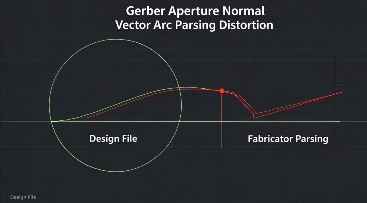
In high-density PCB manufacturing, small geometric errors in Gerber data can become significant production problems. This is especially important for fine-pitch packages such as QFN, BGA, and other components with tight pad-to-pad spacing. A Gerber file may pass standard CAM inspection while the finished PCB still shows unexpected pad displacement.…
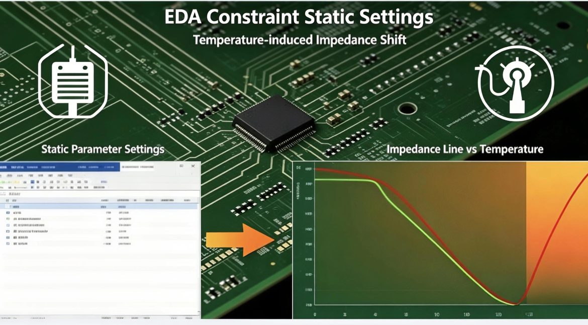
In high-speed PCB design, impedance control is often established through a fixed set of parameters in the EDA environment. Designers typically define target impedance, dielectric thickness, copper thickness, trace width, trace spacing, and dielectric constant at a nominal temperature. This approach may work adequately for products operating near room temperature.…
At first glance, a wiring harness may appear to be nothing more than an organized bundle of wires with connectors attached at the ends. In professional engineering and manufacturing, however, a wire harness is a highly engineered electrical assembly. The selection and integration of every component—from the conductor and insulation…
A wire harness, also known as a cable harness or wiring assembly, is an organized combination of wires, cables, connectors, terminals, protective materials, and other components designed to transmit electrical power and signals efficiently and safely. Depending on the application, a wire harness can contain only a few wires or…
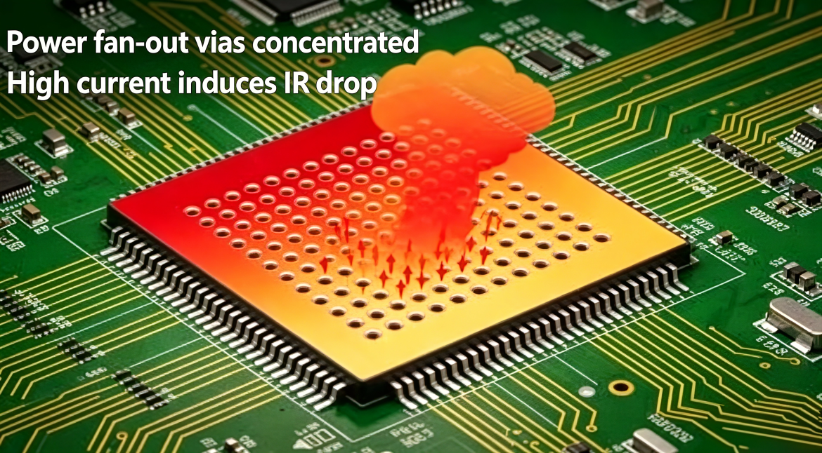
In high-power PCB applications, designers often focus on copper thickness and trace width when evaluating voltage drop. However, these are not the only factors that determine the performance of a power distribution path. A concentrated group of vias can create a significant bottleneck in a high-current PCB power path. Even…