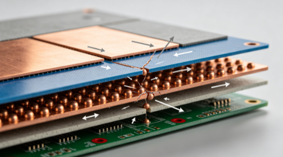
CTE mismatch

CTE Mismatch and BGA Solder Joint Fatigue Failure

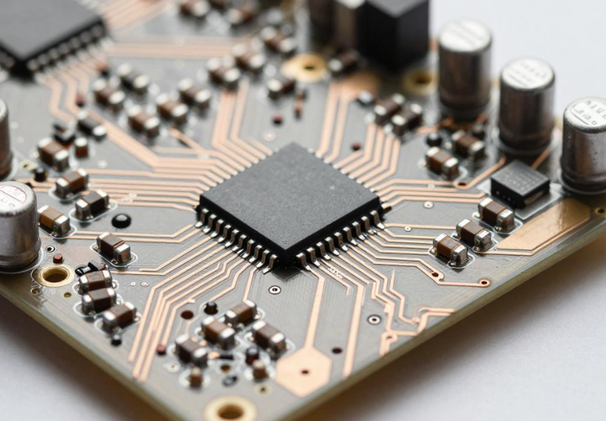
BGA solder joint failures can sometimes occur even when X-ray inspection shows no obvious defect and the soldering process appears to be well controlled. After repeated thermal cycling, cracks may develop at the solder-to-pad or solder-to-package interface, eventually causing intermittent electrical failures or open circuits. One important cause is CTE…
PCB material alternatives

High-Speed PCB Material Selection: Low-Loss FR4 vs High-Frequency Materials

In RF communication, high-speed data acquisition, industrial Ethernet, and other demanding electronic applications, engineers often face a difficult material-selection problem. Traditional high-frequency laminates such as PTFE-based materials and hydrocarbon resin systems can provide excellent electrical performance, but their material costs, fabrication requirements, and supply conditions may increase the overall PCB…
PCB material alternatives

High-Speed PCB Materials: A Guide to Low-Loss PCB Material Selection

When engineers evaluate cost-effective alternatives to premium high-frequency laminates, they often focus primarily on dielectric constant (Dk and Df) and dissipation factor (Dk and Df). While these parameters are essential for high-speed signal design, matching them alone does not guarantee equivalent electrical or manufacturing performance. In real-world PCB development, differences…
PCB material alternatives

High-Speed PCB Materials: How to Choose Low-Loss FR-4 Alternatives

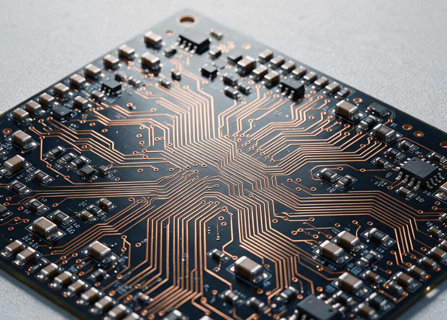
Different electronic products place very different demands on high-speed PCB materials. Consumer communication equipment, industrial control systems, servers, storage backplanes, and RF circuits can differ significantly in signal speed, transmission distance, operating temperature, humidity, insulation requirements, and reliability targets. As a result, there is no single low-cost PCB material that…
PCB copper thickness reduction

Thick Copper PCB Copper Thickness Reduction: Skin Effect and Ripple Current

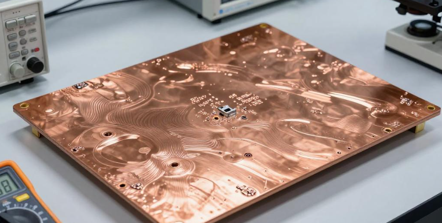
When optimizing PCB copper thickness reduction for a thick copper board, many engineers evaluate current-carrying capability mainly according to DC current and conventional IPC-based calculations. However, this approach may not fully represent the thermal behavior of high-frequency power circuits. In switching power supplies, inverters, motor drives, and other power-conversion systems,…
thick copper PCB

Thick Copper PCB Copper Thickness Reduction: Optimization and Reliability Validation

Reducing copper thickness in a thick copper PCB is a systematic engineering process rather than a simple material change. It involves electrical simulation, PCB design optimization, prototype fabrication, load testing, reliability evaluation, and mass-production monitoring. Skipping any of these steps can introduce long-term risks that may not be visible during…
PCB copper thicknes

Portable Energy Storage 4-Layer PCB Copper Thickness and Current-Carrying Selection

For portable energy storage systems, choosing the right copper thickness is critical to balancing current-carrying capacity, thermal performance, manufacturability, cost, and product size. A common design mistake is to use heavy copper throughout the entire board simply to increase current capacity. While this may provide additional conductor cross-section, it can…