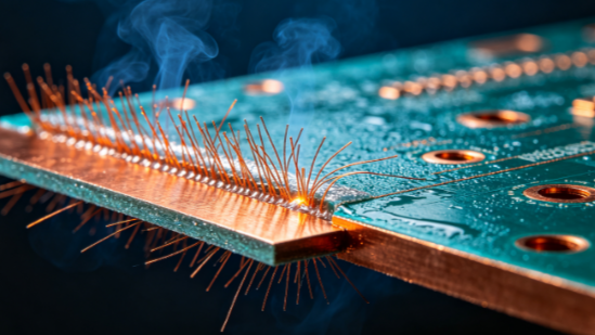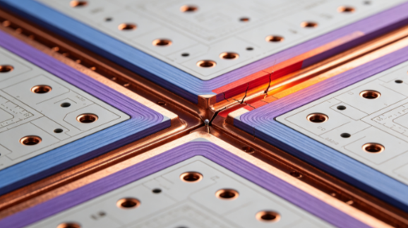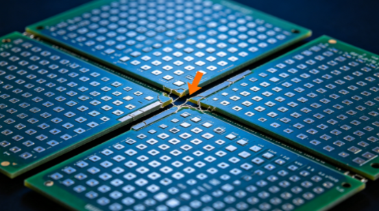
Copper whisker growth

Copper Whisker Growth: Causes, Mechanisms, and PCB Reliability Risks

Copper whisker growth is an easily overlooked reliability issue in advanced PCB manufacturing, particularly in thin-copper, fine-pitch, and high-density BGA applications. Unlike conventional surface oxidation or ionic migration, copper whiskers are filament-like metallic structures that can develop from a copper surface under specific stress and microstructural conditions. If they extend…
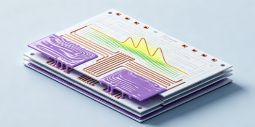
prepreg resin flow

Prepreg Resin Flow and Its Impact on PCB Impedance

In multilayer PCB manufacturing, engineers usually calculate impedance based on trace width, copper thickness, dielectric thickness, and dielectric constant. However, the actual pressed structure can differ from the nominal stackup because prepreg resin flow changes the final dielectric thickness during lamination. This is especially important for impedance-controlled and high-speed PCBs.…
PCB thickness tolerance

PCB Thickness Tolerance and Its Impact on Impedance Consistency

In high-speed multilayer PCB manufacturing, engineers often focus on trace width, copper thickness, dielectric constant, and etching compensation when controlling impedance. However, PCB thickness tolerance can also have a significant influence on impedance consistency because changes in the pressed dielectric structure directly affect the distance between signal traces and their…
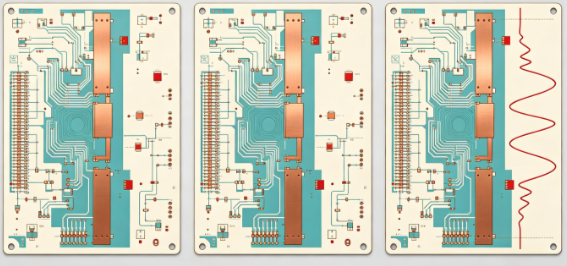
signal integrity

Differential Pair Reference Plane: How It Affects PCB Signal Integrity

In high-speed PCB design, engineers often focus on differential impedance, trace width, via structures, and stackup configuration when troubleshooting signal-integrity problems. However, one issue that is sometimes overlooked is the continuity of the reference plane beneath the differential pair. A slot, copper void, thermal-relief opening, or other discontinuity underneath a…
via wall roughness

Via Wall Roughness in High-Frequency PCBs: Causes of Signal Loss

In high-frequency PCB applications, via quality can directly affect signal integrity, insertion loss, and impedance consistency. This becomes increasingly important in RF, high-speed digital, and millimeter-wave designs, where even small discontinuities in the signal path can contribute to measurable transmission loss. When a high-frequency differential pair passes through a plated…
stackup misalignment

HDI Stackup Misalignment: Causes, Risks, and Reliability Control

In high-density interconnect (HDI) PCB manufacturing, stackup misalignment is more than a cosmetic dimensional deviation. Even a small layer shift can affect microvia geometry, solder-joint reliability, impedance continuity, and thermal-mechanical stress distribution. For example, when a customer reports an unexpected increase in BGA solder-joint failures after assembly, the root cause…