
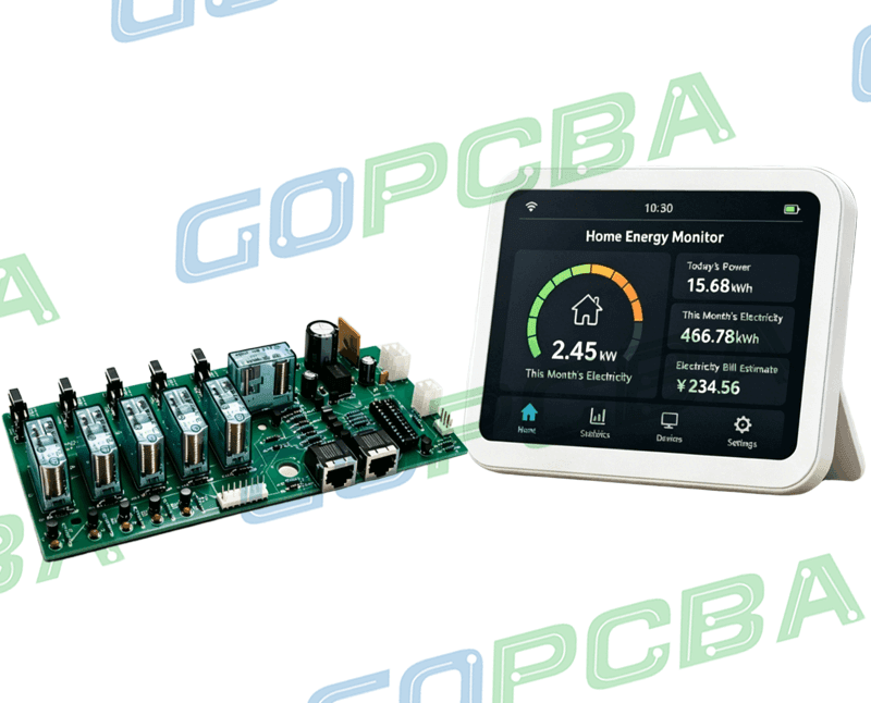
PCB Antenna Board Panelization: What the Sample Leaves Undecided The first run was twenty boards, built to prove the design. By the time the order grew to five hundred, the program had been edited twice and one driver chip had been replaced with a substitute. The question that always follows…
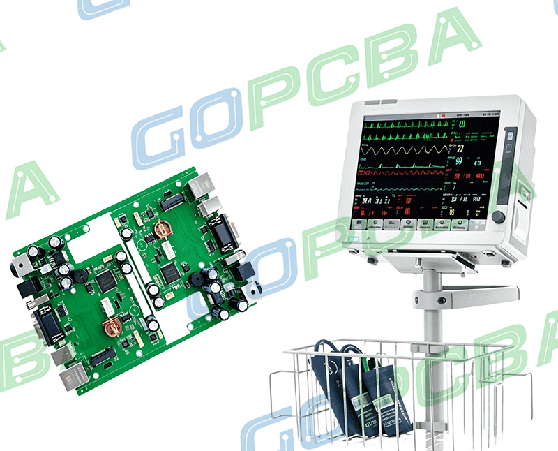
PCB Antenna Board Wave Soldering: What the Sample Leaves Undecided A lot passed inspection and shipped. Three weeks later a customer reported joints that had cracked in the field, and the review that followed was not about the solder alone: it ended at a decision taken long before the line…
PCB Antenna Board Surface Finish: From Sample to Mass Production Two quotations arrive for the same board. One is cheaper, one is more expensive, and the documents look almost identical. The difference usually hides in details nobody discussed: how PCB antenna board surface finish is handled, which checks are recorded,…
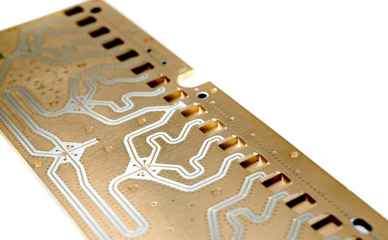
What Is a High-Frequency PCB? A High-Frequency PCB is a printed circuit board designed to transmit and process high-frequency electrical signals while maintaining stable electrical performance, controlled impedance, and low signal loss. High-frequency PCBs are commonly used in applications involving RF, microwave, wireless communication, radar, satellite communication, automotive sensing, medical…
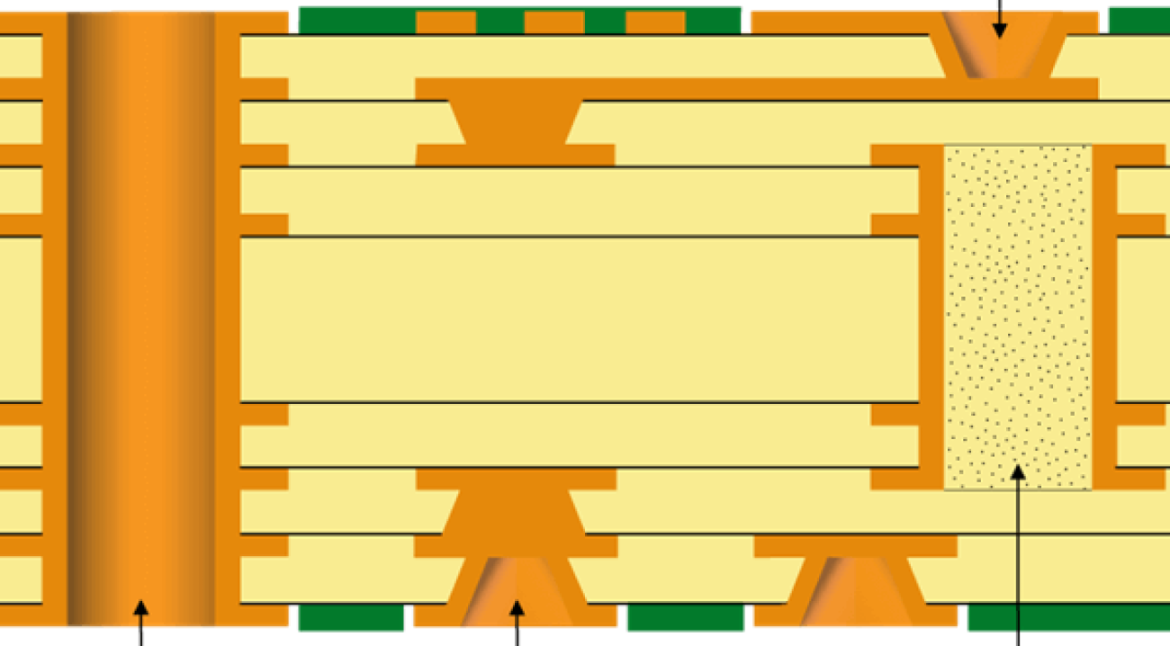
What Is a Microvia PCB? A Microvia PCB is a printed circuit board that uses extremely small vias to create high-density interconnections between PCB layers. Microvias are particularly important in high-density electronic products where conventional through-holes would consume too much routing space. In PCB manufacturing, a microvia is generally understood…
What Are Blind and Buried Via PCBs? A Blind and Buried Via PCB is a printed circuit board that uses blind vias, buried vias, or both to establish electrical connections between different circuit layers while maximizing available board space. In a conventional multilayer PCB, a plated through-hole (PTH) typically extends…
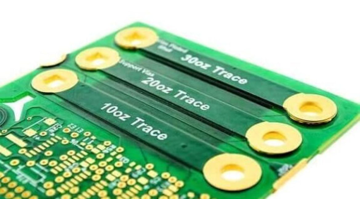
What Is a Heavy Copper PCB? As the name suggests, a Heavy Copper PCB is a printed circuit board manufactured with significantly thicker copper than a standard PCB. In conventional PCB products, copper thickness is commonly around 0.5 to 2 oz, equivalent to approximately 17.5 to 70 μm. When the…
What Is a Low-Loss PCB? A Low-Loss PCB is a printed circuit board designed and manufactured to minimize signal attenuation, dielectric loss, conductor loss, and other sources of transmission loss. These boards are particularly important in high-speed and high-frequency electronic systems where maintaining signal quality over the entire transmission path…
What Is a Taconic PCB? A Taconic PCB is a printed circuit board manufactured using high-performance laminate materials developed by Taconic’s Advanced Dielectric division. These materials are engineered primarily for demanding RF, microwave, and high-speed digital applications where conventional PCB materials may not provide sufficient electrical or thermal performance. Taconic…
What Is a Halogen-Free PCB? A Halogen-Free PCB is a printed circuit board manufactured without intentionally using halogen-based materials, particularly halogenated flame retardants. Halogens are a group of chemical elements that includes: Fluorine (F) Chlorine (Cl) Bromine (Br) Iodine (I) Astatine (At) Traditional PCB materials may contain brominated flame retardants…