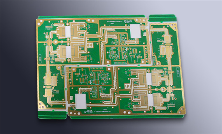
High-Frequency PCB for Automotive Radar Systems With the rapid development of Advanced Driver Assistance Systems (ADAS) and autonomous driving technology, automotive radar has become one of the most essential sensing technologies in modern intelligent vehicles. Compared with cameras, radar continues to work reliably in rain, snow, fog, and at night,…
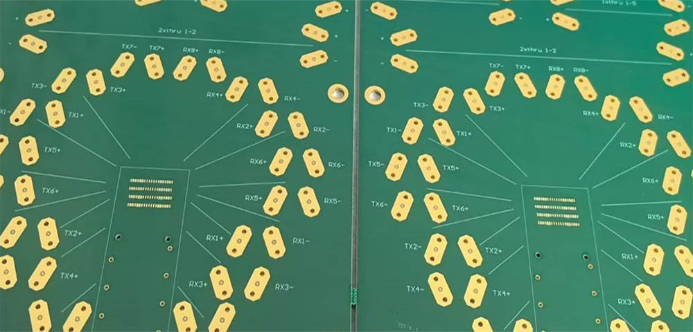
Automotive PCB Manufacturing: Materials and Quality Control Vehicle electronics no longer sit in a comfortable cabin. Control units, radar modules, and battery management boards face heat, cold, vibration, and moisture for many years. That environment changes what a PCB must survive, not just what it must do. Manufacturing decisions that…
Downhole PCB Material Choices for Detection Equipment Downhole detection equipment works where humidity, dust, vibration and heat arrive together. Boards inside these tools must survive transport, installation and years of service underground. Material choice therefore shapes reliability more than any single assembly step. This review explains how substrate, copper, solder…
Multilayer High-Speed PCB Prototyping for Server Boards Server motherboards carry processors, memory, storage links, and power delivery in a small area. A prototype must prove that this dense design can be built and measured before volume begins. The work starts with the stack-up, not with the drill file. Each layer…
High-Speed PCB Manufacturing for Signal Integrity Testing High-speed boards fail for reasons that rarely appear in the schematic. Trace width, dielectric thickness, copper roughness and via geometry all shift the electrical behavior of a finished board. A fabricator that controls these variables gives the test lab a stable platform. A…
Solar Backsheet PCB Production and Manufacturing Solar backsheet PCBs carry power and control signals inside photovoltaic modules for years of outdoor service. Production planning therefore starts with the environment, not with the machine list. Heat, moisture, ultraviolet light and daily temperature swings all act on the same laminate. A board…
PCB Back Drilling: Process, Benefits and Applications A plated through-hole that runs the full board thickness leaves copper below the last connected layer. That leftover section is a via stub. At low speeds it does little harm. At multi-gigabit rates it acts as a stub antenna and distorts the channel.…
High Layer Count PCB Manufacturing: 20+ Layer Process A 20-layer board is not a 6-layer board with more copper. Each added pair of layers stacks another registration risk, another lamination cycle, and another chance for resin flow to move things. Buyers comparing quotes on a high layer count build should…
PCB Warpage in Manufacturing – Causes, Impact & Proven Solutions In PCB manufacturing, board flatness directly affects product quality, assembly efficiency, and long‑term reliability. With the trend toward higher density, miniaturisation, and high performance, PCB warpage has become a critical issue in design, fabrication, and SMT assembly. Whether in consumer…
PCB High‑Temperature Deformation – Causes, Impact & Prevention Strategies With the rapid growth of automotive electronics, industrial control, new energy systems, communication equipment, and high‑power electronics, PCBs must not only meet electrical performance requirements but also provide excellent mechanical stability and heat resistance. However, during PCB manufacturing, SMT assembly, and…