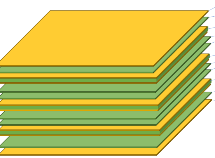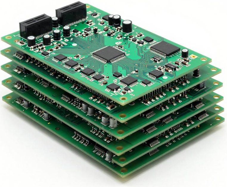
In many PCB designs, excessive layer count does not necessarily come from having too many signal layers. It can also result from unnecessarily separating power and ground planes. A common design habit is to assign one dedicated layer to each voltage rail or to physically separate every ground domain. While…
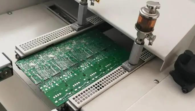
Many engineers evaluate redundant-layer reduction primarily from the perspective of material savings and lower PCB costs. However, its potential value extends beyond cost reduction. When properly engineered, reducing unnecessary layers can simplify the PCB manufacturing process, optimize the stackup, improve process stability, and reduce manufacturing risks during mass production. For…
Reducing redundant PCB layers is not simply a matter of removing unused copper layers. It is a formal design change that can affect signal integrity, power distribution, mechanical strength, thermal behavior, manufacturability, and long-term reliability. In practical projects, improper PCB layer reduction can create unexpected problems. A design may experience…
Outdoor gateways serve as edge IoT devices for data acquisition, processing, and communication. They are often installed in outdoor cabinets and exposed to demanding environmental conditions, including wide temperature fluctuations, high humidity, condensation, lightning-induced surges, and the coexistence of digital and RF signals. Compared with four-layer boards, a 6-layer PCB…
Outdoor gateways often integrate DDR memory interfaces, Gigabit Ethernet, Sub-GHz or 5G wireless circuits, and other high-speed digital and RF interfaces on the same PCB. This combination creates a challenging routing environment in which high-speed differential routing, return-path continuity, impedance control, and electromagnetic compatibility (EMC) must be considered together. For…
During hardware product development and iteration, industrial, medical, RF, power, and other specialized applications may require special-process PCB technologies such as thick copper, embedded resistors, resin-filled vias, metal-core structures, or high-frequency materials. When estimating project costs, engineers often focus on the price of the laminate or copper material while overlooking…
When engineers receive a quotation for a PCB with uncommon materials or special manufacturing requirements, they often focus on basic specifications such as material, layer count, and board dimensions. However, the quoted unit price may not include every engineering, testing, tooling, expedited-production, packaging, or logistics cost. This is particularly important…
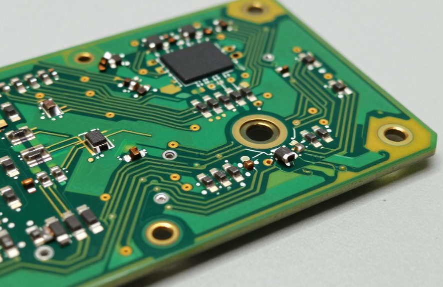
In PCB mass production, surface finishing is one of the critical process areas affecting solderability, appearance, electrical performance, and long-term reliability. Common defects such as pad oxidation, poor solderability, uneven coating thickness, gold layer peeling, discoloration, and corrosion are often related not only to individual process failures but also to…
DFM (Design for Manufacturability) review is an essential step before a multilayer PCB enters production. Among the most common DFM issues are problems related to the solder mask layer. A PCB may perform normally during prototyping but develop solder mask blistering, ink peeling, opening misalignment, or solder mask bridge failure…
During multilayer PCB mass production, solder mask defects can appear in large numbers, including blistering, delamination, ink peeling, pinholes, cracking, and localized exposed copper. When these problems occur, it is tempting to immediately blame the solder mask ink or the PCB manufacturer. However, solder mask failure is rarely caused by…