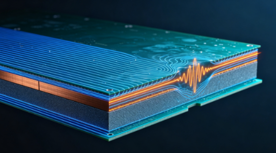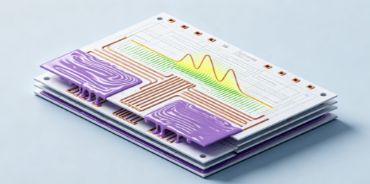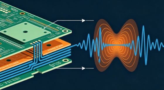
A high-speed server PCB can pass signal integrity simulation and still experience unexpected failures during laboratory testing. One common cause is power plane resonance, which can create localized voltage fluctuations in the power distribution network (PDN) and indirectly disturb high-speed signal paths. During the debugging of an 8-layer server board,…

During an EMI interference investigation for a power electronics PCB, a noticeable emission increase was observed around 300 MHz. Cross-sectional analysis revealed a small copper area on an inner layer that was electrically floating and positioned very close to an adjacent signal trace. This type of structure is often overlooked…
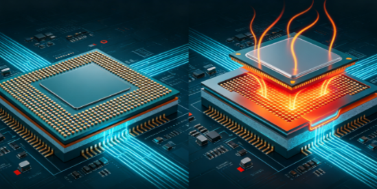
In high-density PCB assemblies, removing copper beneath a BGA package is sometimes considered a way to improve solder-joint reliability or provide more routing space. However, copper removal does not automatically improve thermal performance. In many cases, the result depends on where the copper is removed, which layers are affected, and…
As PCB operating frequencies continue to increase, material stability becomes increasingly important. This is especially true for 6G PCB designs, millimeter-wave radar, high-speed communication equipment, and other RF applications where even small changes in dielectric properties can affect impedance, phase, insertion loss, and overall system performance. After reflow or other…
Microcracks formed during PCB lamination may remain invisible immediately after manufacturing but gradually develop under repeated thermal cycling. This is particularly important for multilayer PCBs with BGA packages, where differences in thermal expansion between copper, laminate, prepreg, and package structures can create repeated mechanical loading. For example, after thermal cycling…
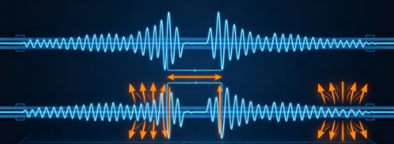
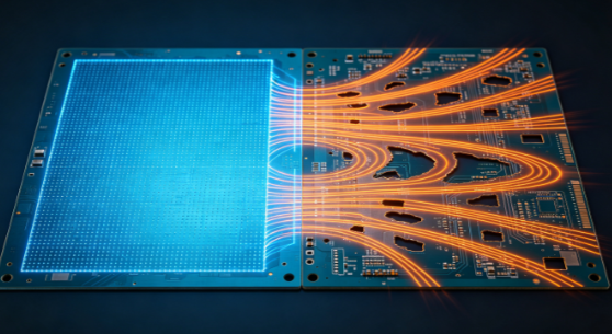
When a differential pair suddenly crosses a discontinuity in its reference plane—for example, a split plane, a thermal pad clearance, a power-island boundary, or a large void in an internal reference layer—the electromagnetic field around the transmission path can change significantly. This discontinuity can increase coupling to adjacent traces and…
Large-area copper voids in a PCB ground plane may appear to save material, reduce capacitance, improve manufacturability, or accommodate thermal and mechanical requirements. However, in high-speed and RF designs, excessive voiding can significantly change the electrical behavior of the reference structure. A continuous ground plane provides a low-impedance return path…
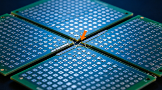
In fine-pitch PCB assembly, the solder mask bridge between adjacent pads can become one of the weakest structural features on the board. This is particularly important for BGA packages with very small pad spacing, where the available solder mask bridge width may be only a few tens of micrometers. When…
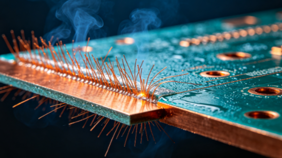
Copper whisker growth is an easily overlooked reliability issue in advanced PCB manufacturing, particularly in thin-copper, fine-pitch, and high-density BGA applications. Unlike conventional surface oxidation or ionic migration, copper whiskers are filament-like metallic structures that can develop from a copper surface under specific stress and microstructural conditions. If they extend…
In multilayer PCB manufacturing, engineers usually calculate impedance based on trace width, copper thickness, dielectric thickness, and dielectric constant. However, the actual pressed structure can differ from the nominal stackup because prepreg resin flow changes the final dielectric thickness during lamination. This is especially important for impedance-controlled and high-speed PCBs.…