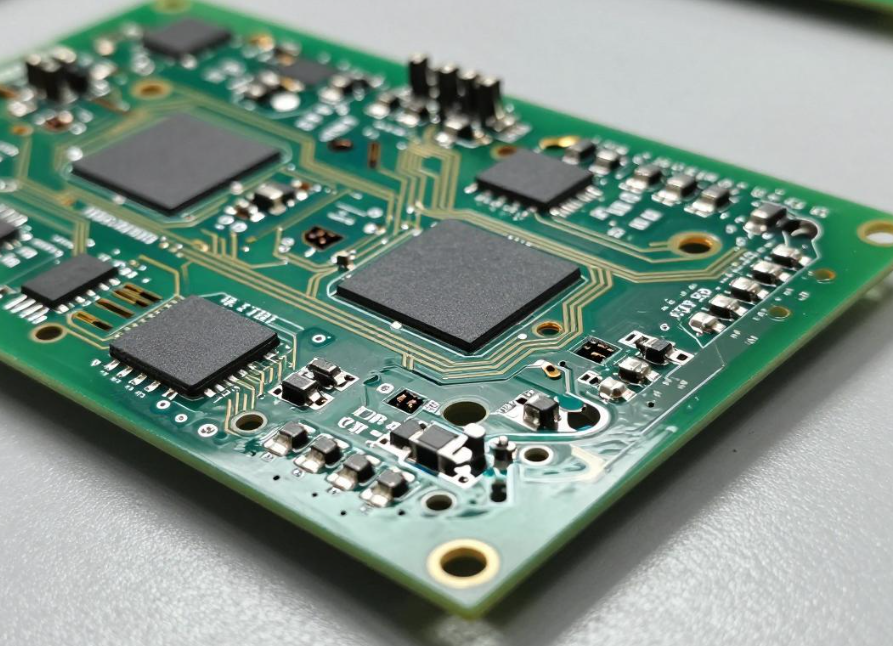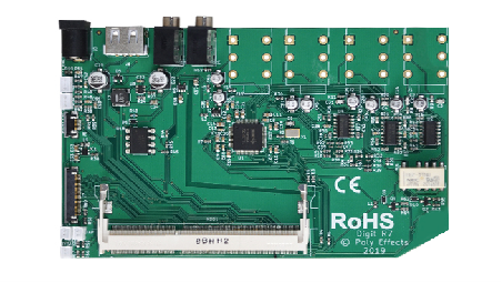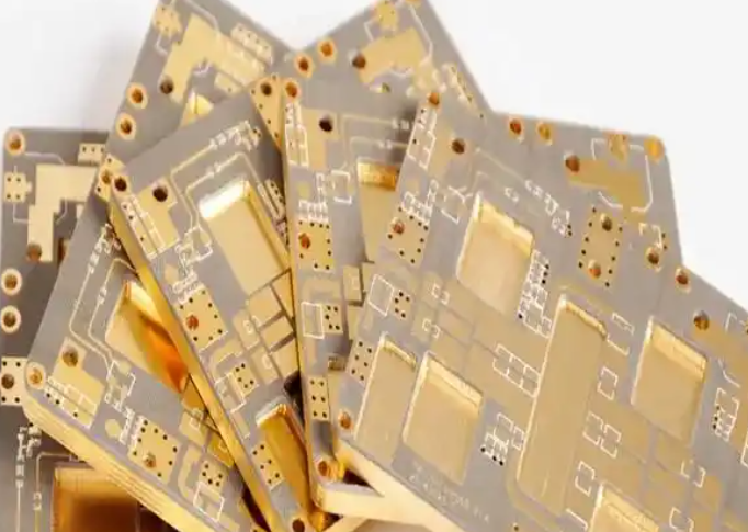
Many hardware engineers attribute gold thickness uniformity entirely to the PCB manufacturer’s plating process. However, PCB layout, copper distribution, pad geometry, and panelization can also influence the plating environment and amplify local variation. A design that creates significant differences in exposed surface area, copper distribution, panel position, or solution accessibility…
Even after PCB design optimization and process control are completed, high-volume ENIG PCB production still requires systematic inspection and validation to prevent nonconforming boards from entering assembly. Gold thickness uniformity is particularly important because many thickness variations cannot be identified through visual inspection alone. A PCB may have an acceptable…
OSP, or Organic Solderability Preservative, is widely used in consumer electronics, industrial control equipment, communication boards, and other applications because it provides a relatively flat soldering surface, supports fine-pitch BGA and QFN assembly, and can offer a cost-effective surface-finish solution. However, a common production problem is that prototype boards may…
The oxidation resistance of an OSP PCB is often attributed entirely to the PCB manufacturer’s surface-finishing process. However, PCB layout, panelization, packaging, transportation, storage, and assembly conditions can all affect the final performance of an OSP surface finish. Some PCB designs can create unfavorable manufacturing conditions from the beginning. Even…
During the mass-production stage of industrial control, energy-storage, automotive, and export-oriented consumer electronics projects, engineers and procurement teams often make a simple assumption: a halogen-free PCB means a circuit board that contains absolutely no halogens. In practice, this definition is more nuanced. A PCB can be manufactured with a halogen-free…
Once a project requires a halogen-free PCB, engineers often focus primarily on glass transition temperature (Tg) when comparing laminate materials. However, Tg is only one part of the material selection process. Thermal decomposition temperature (Td), Z-axis coefficient of thermal expansion (Z-axis CTE), moisture absorption, and comparative tracking index (CTI) can…
Batch delivery does not mean that a halogen-free PCB project has been successfully implemented. Many hardware teams consider PCB arrival and basic electrical continuity testing to be the end of the project. However, without systematic documentation review, material verification, sampling inspection, and reliability validation, problems may only appear during large-scale…
During the early stages of PCB development, hardware engineers sometimes specify a custom finished board thickness based primarily on mechanical clearance. Values such as 1.4 mm, 1.8 mm, or 2.2 mm may be selected even when the application does not require a non-standard thickness. Although a custom thickness may appear…
In DDR, MIPI, Ethernet, and RF PCB projects, changing a non-standard board thickness to a standard thickness can create a significant risk of impedance control problems. For example, directly changing a 1.7 mm non-standard PCB to a 1.6 mm standard thickness without reviewing the stackup may alter dielectric thickness and…
When converting a multilayer PCB from a non-standard finished thickness to a standard thickness, the key is to redesign the combination of PCB core and prepreg (PP) materials. Many engineers focus only on the final thickness value while overlooking resin flow, stackup symmetry, CTE compatibility, and lamination behavior. As a…