PCB Design

PCB Design Safety Clearance: Electrical and Mechanical Spacing Guidelines

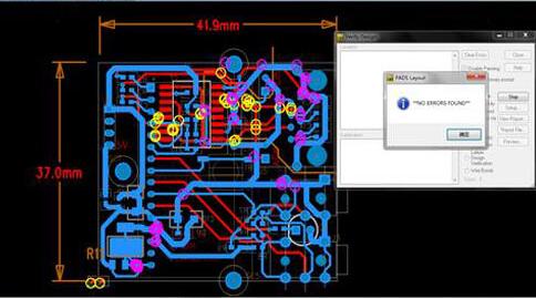
In PCB Design, safety clearance is one of the fundamental considerations for electrical performance, manufacturing reliability, and mechanical compatibility. Designers need to consider many different types of spacing, including the distance between traces, pads and vias, copper and the board edge, silkscreen and pads, components and neighboring structures, and components…
PCB Quality Control

Common PCB Defects: Causes, Solutions and Quality Control Guide

Printed circuit boards are essential components of virtually every electronic product. They provide the electrical and mechanical foundation for connecting and supporting electronic components, making PCB quality directly related to the performance, reliability, and service life of the final product. During the PCB Manufacturing process, numerous manufacturing variables must be…
PCB Manufacturing Process

PCB Manufacturing Process: A Complete Guide to Single-Sided, Double-Sided and Multilayer PCBs

The PCB Manufacturing Process varies according to the board type, layer count, material system, design complexity, and manufacturing technology. Although the basic principles of PCB fabrication have remained relatively stable, advances in imaging, drilling, plating, lamination, surface treatment, and inspection technologies have significantly changed modern production methods. A simple single-sided…
Power Integrity

PCB Power Integrity Design: PDN, Decoupling and Power Plane Optimization

As electronic products continue to evolve toward higher performance, smaller form factors, and greater integration, Power Integrity has become an essential consideration in modern PCB Design. High-performance processors, FPGAs, memory devices, networking ICs, and other high-pin-count components often operate with multiple power rails and increasingly low supply voltages. As operating…
Microvia Drilling

Microvia Formation in PCB Manufacturing: Laser Drilling vs. Mechanical Drilling

As electronic products continue to become smaller, thinner, and more highly integrated, circuit designers need increasingly compact interconnection structures. Microvia technology has therefore become an important part of modern high-density PCB manufacturing, particularly for high-density interconnect (HDI) boards. A microvia can be produced using several different manufacturing technologies. The two…
Printed Circuit Board (PCB)

PCB History and Manufacturing: From Early Circuit Boards to Multilayer PCBs

The development of the Printed Circuit Board (PCB) fundamentally changed the electronics industry. Before the invention of the PCB, electronic components were primarily interconnected using point-to-point wiring. As electronic products became smaller, more complex, and more reliable, traditional wiring methods could no longer meet the requirements of mass production. The…
PCB Lamination Process

Multilayer PCB Lamination: Process, Materials and Quality Control

As electronic products continue to become smaller, faster, and more functionally integrated, printed circuit boards are evolving from simple single-sided and double-sided structures toward increasingly sophisticated multilayer configurations. A Multilayer PCB can accommodate a large number of signal, power, and ground connections within a relatively compact board structure. However, as…
HDI Circuit Board

HDI PCB for Mobile Devices and High-End Servers

As smartphones, tablets, and other mobile electronic devices continue to become smaller, thinner, lighter, and more portable, the available space inside their mainboards is becoming increasingly limited. At the same time, consumers expect these devices to provide more functions and higher performance. This trend has increased demand for HDI PCB…