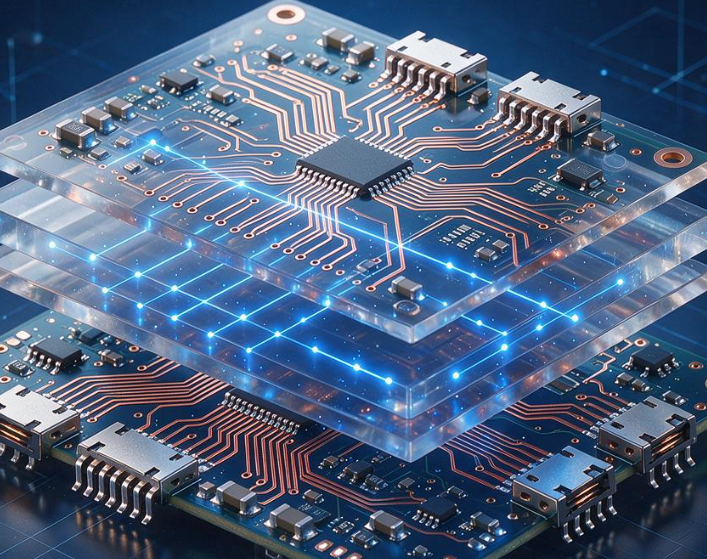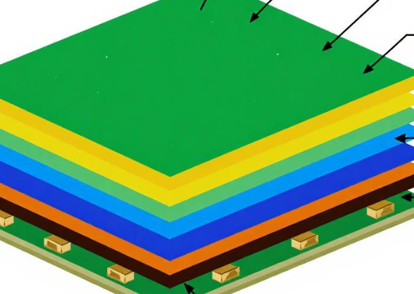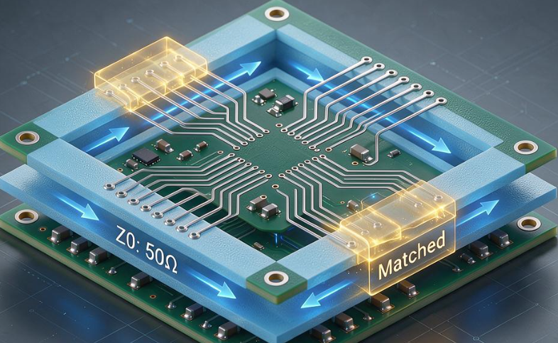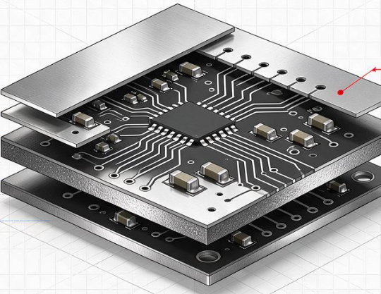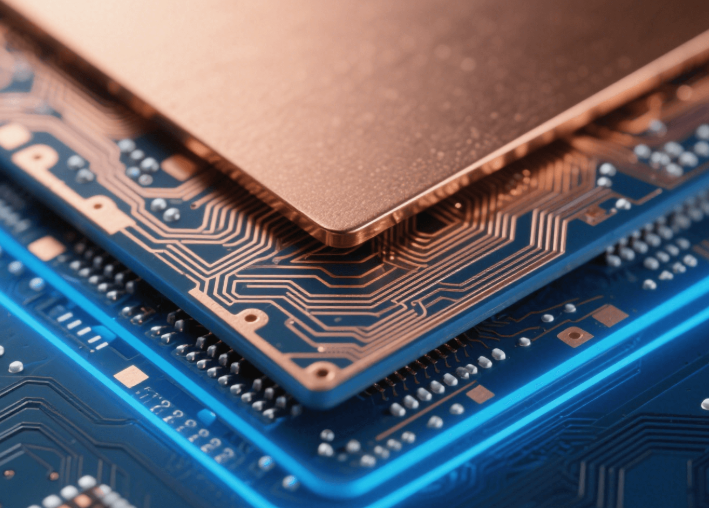
In multilayer PCB manufacturing, prepreg is an essential material used to bond copper layers and form the dielectric structure of the finished board. When optimizing a PCB Stackup, many projects face a difficult balance between electrical performance, material cost, manufacturing yield, and long-term reliability. Two common approaches can create unnecessary…
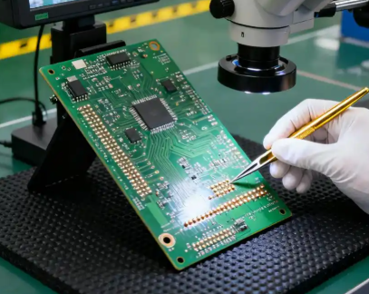
PCB Prototype production is typically carried out in small quantities to verify circuit performance, mechanical fit, and manufacturing feasibility. At this stage, manufacturers can often accommodate designs that are not fully optimized for automated, high-volume production. However, a design that works well for prototypes may encounter significant problems when transferred…
In high-speed circuit design for a Multilayer PCB, many engineers focus primarily on trace width when calculating controlled impedance. However, trace width is only one part of the transmission-line structure. The dielectric thickness, dielectric properties, copper geometry, and reference-plane configuration all influence the final impedance. If the dielectric system is…
In multilayer PCBs, many inner-layer signal traces use a Stripline configuration, in which the signal conductor is located between two reference planes. Unlike a surface microstrip, the electrical environment of a stripline is determined by the dielectric layers and reference planes above and below the signal. Because both dielectric layers…
Many engineers complete impedance simulation, determine trace widths, and finalize the stackup based on nominal material parameters. However, significant impedance variation may only become apparent after mass production begins. Impedance can vary from board to board and even across different regions of the same PCB. Although trace etching and copper…
The cost of correcting impedance problems increases rapidly as a PCB project moves from prototyping to mass production. During the prototype stage, dielectric-related impedance issues can often be addressed by modifying the stackup or material selection. Once a product enters volume production, however, an impedance failure caused by dielectric variation…
Switching from conventional PCB materials to Halogen-Free PCB materials is not simply a matter of changing the laminate specification in the BOM. Halogen-free laminates can have different resin systems, glass-fiber characteristics, thermal behavior, drilling performance, and lamination requirements compared with conventional FR-4 materials. A PCB design that performs normally during…
PCB Manufacturing is the process of converting a PCB design into a physical, functional printed circuit board. It involves a series of controlled manufacturing operations that create conductive patterns, dielectric structures, plated interconnections, protective coatings, and finished surface features on a PCB. A printed circuit board provides both mechanical support…
Electronic products have become an essential part of modern life. From smartphones and wearable devices to smart home products, new energy systems, telecommunications equipment, medical devices, automotive electronics, and industrial automation, electronic technology powers many of the products and systems around us. However, developing a reliable electronic product requires expertise…
What Is PCB Design? PCB Design is the process of converting an electronic circuit concept and schematic into a physical printed circuit board (PCB) that can be manufactured, assembled, tested, and used reliably in its intended application. A PCB design integrates electrical circuits, component placement, copper routing, layer stackup, mechanical…