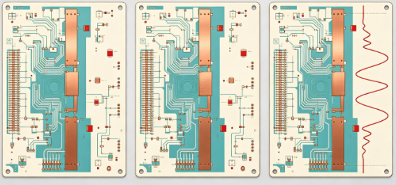
In high-speed multilayer PCB manufacturing, engineers often focus on trace width, copper thickness, dielectric constant, and etching compensation when controlling impedance. However, PCB thickness tolerance can also have a significant influence on impedance consistency because changes in the pressed dielectric structure directly affect the distance between signal traces and their…

In high-speed PCB design, engineers often focus on differential impedance, trace width, via structures, and stackup configuration when troubleshooting signal-integrity problems. However, one issue that is sometimes overlooked is the continuity of the reference plane beneath the differential pair. A slot, copper void, thermal-relief opening, or other discontinuity underneath a…
In high-frequency PCB applications, via quality can directly affect signal integrity, insertion loss, and impedance consistency. This becomes increasingly important in RF, high-speed digital, and millimeter-wave designs, where even small discontinuities in the signal path can contribute to measurable transmission loss. When a high-frequency differential pair passes through a plated…
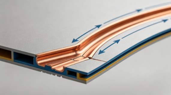
A V-Cut that is cut too deeply can significantly weaken a PCB panel and increase the risk of cracking, warpage, or edge damage during SMT assembly and reflow. When a PCB develops cracks after reflow, the problem is not necessarily caused by soldering temperature alone. In some cases, the root…
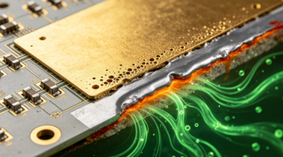
A darkened gold surface, poor solderability, or weakened BGA solder joints does not always indicate oxidation of the gold layer. In some ENIG failures, the underlying nickel-phosphorus layer is the actual region where corrosion initiates. During failure analysis, localized corrosion may appear as pits, voids, discoloration, or interfacial separation beneath…
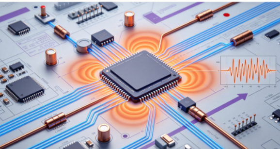
When a BGA device powers up and multiple I/O signals switch simultaneously, a short-duration voltage spike may appear on the power or ground pins. In severe cases, the transient can disturb the power-on-reset circuit and cause an unexpected system reset. Interestingly, two identical ICs on the same PCB can behave…
In high-density interconnect (HDI) PCB manufacturing, stackup misalignment is more than a cosmetic dimensional deviation. Even a small layer shift can affect microvia geometry, solder-joint reliability, impedance continuity, and thermal-mechanical stress distribution. For example, when a customer reports an unexpected increase in BGA solder-joint failures after assembly, the root cause…
BGA solder joint failures can sometimes occur even when X-ray inspection shows no obvious defect and the soldering process appears to be well controlled. After repeated thermal cycling, cracks may develop at the solder-to-pad or solder-to-package interface, eventually causing intermittent electrical failures or open circuits. One important cause is CTE…
In high-speed backplane and multilayer PCB designs, engineers often focus on stackup structure, dielectric thickness, trace width, and Dk when controlling impedance. However, a less obvious factor can also affect high-speed transmission: copper thickness changes along the signal path. Consider a 40G backplane design with 50 Ω single-ended and 100…
In RF communication, high-speed data acquisition, industrial Ethernet, and other demanding electronic applications, engineers often face a difficult material-selection problem. Traditional high-frequency laminates such as PTFE-based materials and hydrocarbon resin systems can provide excellent electrical performance, but their material costs, fabrication requirements, and supply conditions may increase the overall PCB…