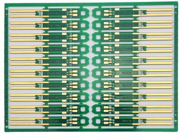
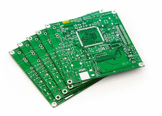
How Are PCBs Manufactured? The Full Production Flow A bare board starts as copper-clad laminate and leaves as a tested circuit. Between those points sit imaging, etching, lamination, drilling, plating, masking and inspection. Each step changes the panel in ways the next step cannot undo. That is why the flow…
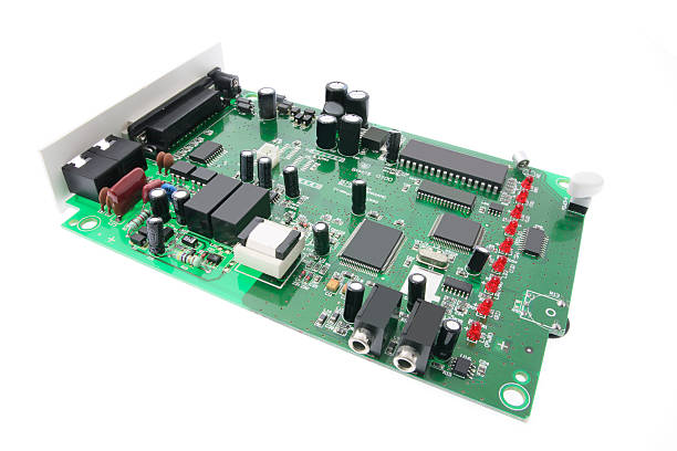
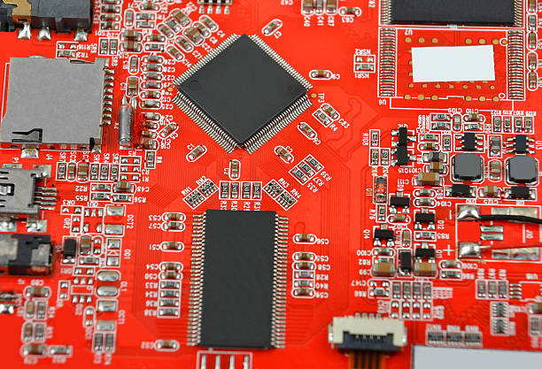
PCB Assembly (PCBA): Process, Types, Testing, Standards & Manufacturing Guide PCB assembly (PCBA) is the process of mounting and soldering electronic components onto a printed circuit board (PCB) to create a functional electronic assembly. A bare PCB provides the conductive pathways, pads, vias, and mechanical foundation needed to interconnect circuits,…
The PCB Manufacturing Process consists of a series of carefully controlled operations that transform raw PCB materials into precisely sized and shaped panels ready for subsequent fabrication processes. Although different PCB types may require different manufacturing routes, the basic principles of material preparation, panel cutting, dimensional control, and initial forming…
PCB Production Files: Gerber, Drill and Manufacturing Data A production package is the handoff between design intent and the factory floor. It carries the artwork, the hole data and the written requirements that operators, engineers and inspectors all work from. When that package is complete, the job moves without questions.…
Professional PCB Manufacturing: Technology and Quality Professional PCB manufacturing is a chain of controlled steps, not one machine. Material selection, imaging, drilling, plating, lamination and inspection each change the finished board. A capable factory links these steps with process data and engineering review. Buyers should judge a supplier by how…
High-Precision Multilayer PCB Manufacturing Process A high-precision multilayer board is not defined by its layer count alone. It is defined by how tightly the factory controls layer registration, hole position, copper thickness, dielectric spacing and surface finish. Those controls decide whether vias connect, whether impedance holds and whether the panel…
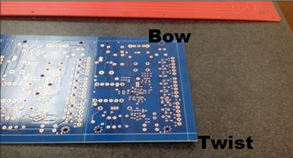
PCB flatness is an important quality requirement throughout PCB Manufacturing and assembly. As electronic products become smaller, thinner, and more highly integrated, the dimensional stability and flatness of printed circuit boards have become increasingly critical. During automated surface-mount assembly, excessive PCB Warpage can cause positioning errors, poor solder paste printing,…
Blind and Buried Via PCB Manufacturing: Key Challenges A blind via reaches from an outer layer to an inner layer without crossing the full board. A buried via connects inner layers only and never appears on either surface. Both structures free routing space and shorten signal paths in dense designs.…
How to Repair a Keyboard PCB: Keyboard PCB Repair, Troubleshooting & Rework Guide The development of electronic technology has transformed nearly every modern product and application. From early computing systems to today’s compact smart devices, each generation of computers has evolved alongside advances in electronics, semiconductor technology, and PCB design.…
Medical PCB Cleaning Standards: Process, Testing & Compliance Flux residue left on a medical board rarely shows up as a visible stain. It sits around component leads, under connectors, and inside vias, where it waits for humidity. The cleaning step decides whether that residue becomes a leakage path months later…